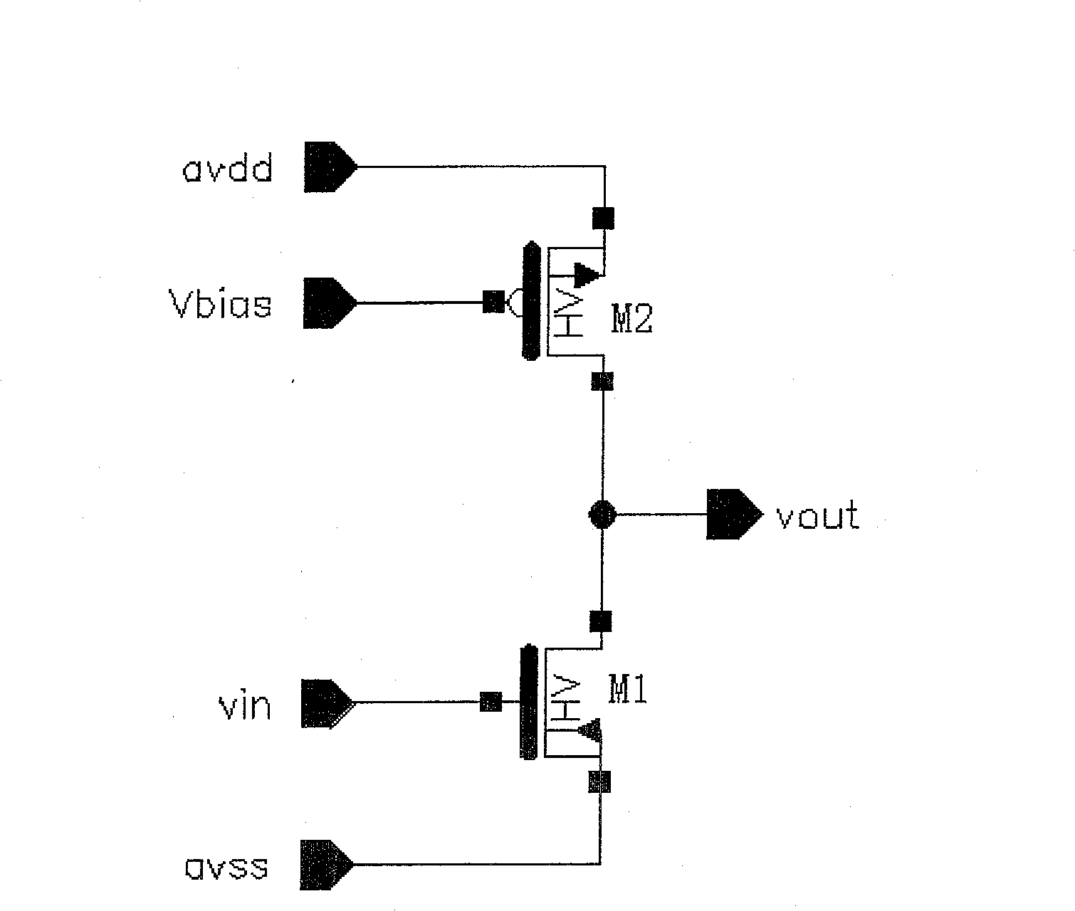
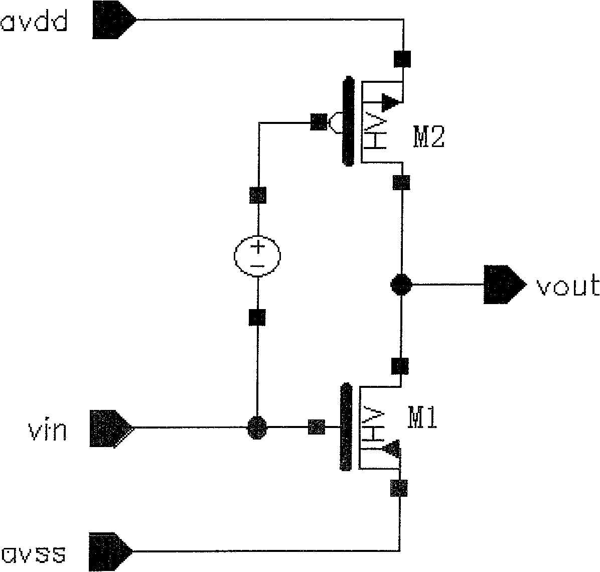
Output circuit of calculation amplifier
A technology for output stage circuits and operational amplifiers, applied in differential amplifiers, DC coupled DC amplifiers, etc., can solve the problems of output stage output efficiency reduction, complex circuit structure, high input impedance, etc., to increase the maximum output current and improve span The effect of guiding and simplifying the circuit
- Summary
- Abstract
- Description
- Claims
- Application Information
AI Technical Summary
Problems solved by technology
Method used
Image
Examples
Embodiment Construction
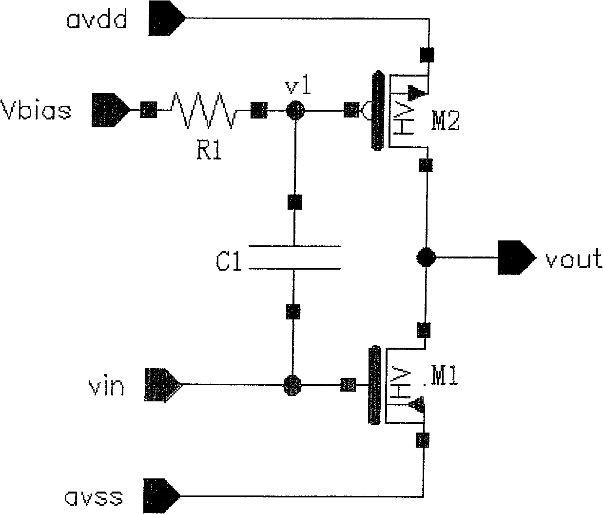
[0015] The output stage circuit of operational amplifier of the present invention can refer to image 3 As shown, it includes two triodes M1 and M2 whose drains are connected together, the drain of the triode M1 and the drain of M2 are used as output terminals, the source of the triode M2 is connected to the power supply terminal, and the source of the triode M1 The pole is grounded, the gate of the triode M1 is used as an input terminal, the gate of the triode M2 is connected to a resistor R1, and the end of the resistor R1 not connected to the triode M2 is used as a voltage bias input terminal, the triode M1 A capacitor C1 is connected between the gate of M2 and the gate of M2.
[0016] The transistor M1 is an NMOS transistor, the transistor M2 is a PMOS transistor, the input terminal vin is connected to the gate of the transistor M1, the source of the transistor M1 is grounded to avss, and the drain of the transistor M1 is connected to the drain of the M2, which toget...
PUM
 Abstract
Description
Claims
Application Information
 - R&D
- Intellectual Property
- Life Sciences
- Materials
- Tech Scout
- Unparalleled Data Quality
- Higher Quality Content
- 60% Fewer Hallucinations
Browse by: Latest US Patents, China's latest patents, Technical Efficacy Thesaurus, Application Domain, Technology Topic, Popular Technical Reports.
© 2025 PatSnap. All rights reserved.Legal|Privacy policy|Modern Slavery Act Transparency Statement|Sitemap|About US| Contact US: help@patsnap.com


