Degradable substrate for flexible optoelectronic device and manufacture method thereof

A technology of optoelectronic devices and substrates, which is applied in the fields of electrical solid-state devices, semiconductor/solid-state device manufacturing, photovoltaic power generation, etc. Light transmittance, crystallinity reduction effect

Inactive Publication Date: 2015-09-30
UNIV OF ELECTRONICS SCI & TECH OF CHINA
View PDF5 Cites 4 Cited by
  • Summary
  • Abstract
  • Description
  • Claims
  • Application Information

AI Technical Summary

Problems solved by technology

However, despite these advantages, there are still many limitations in substituting flexible substrates for rigid substrates, and the fabrication of flexible devices still has many fundamental issues to be resolved.
For example, first of all, due to the low surface energy of flexible substrates compared with rigid substrates, the adhesion of the films to be deposited is relatively poor, and the surface flatness of flexible substrates is far less than that of glass substrates.
Moreover, the electrode materials of organic optoelectronic devices are easily oxidized in an oxygen-containing environment, resulting in a decrease in device performance; organic materials are very sensitive to impurities, oxygen, and water, and are easily contaminated to reduce device efficiency.
In addition, most flexible substrates are non-degradable or have certain toxicity. Therefore, the ecological environment pollution caused by electronic waste is also a problem in the field of flexible optoelectronics.

Method used


Image

  • Degradable substrate for flexible optoelectronic device and manufacture method thereof
  • Degradable substrate for flexible optoelectronic device and manufacture method thereof
  • Degradable substrate for flexible optoelectronic device and manufacture method thereof

Examples


Embodiment 1

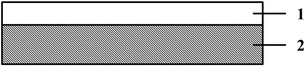
[0106] Such as figure 1 In the substrate structure shown, the flexible substrate 2 is shellac doped with UV-sensitive glue, and the conductive layer 1 is graphene. The preparation method is as follows:

[0107] ① Clean the rigid substrate with surface roughness less than 1nm, and dry it with dry nitrogen after cleaning;

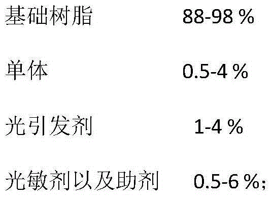
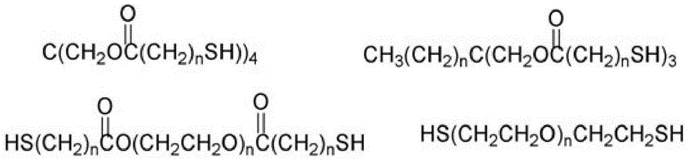
[0108] ② Prepare a flexible substrate by spin coating on a rigid substrate, the flexible substrate is shellac, and the shellac is mixed with a UV-sensitive glue with a mass ratio of 0.3%, and the film thickness is 100 μm. The UV-sensitive glue is A mixed system of free-radical UV-sensitive adhesive and cationic UV-sensitive adhesive, the mass ratio of free-radical UV-sensitive adhesive to cationic UV-sensitive adhesive is 1:10, and the raw material of the free-radical UV-sensitive adhesive includes 88% base Resin, 4% monomers, 4% photoinitiators and 4% photosensitizers and auxiliary agents; the cationic UV-sensitive adhesive raw materials include 98% cation...

Embodiment 2

[0114] Such as figure 1 In the substrate structure shown, the flexible substrate 2 is shellac doped with UV-sensitive glue, and the conductive layer 1 is carbon nanotubes. The preparation method is as follows:

[0115] ① Clean the rigid substrate with surface roughness less than 1nm, and dry it with dry nitrogen after cleaning;

[0116] ② Prepare a flexible substrate by spin coating on a rigid substrate, the flexible substrate is shellac, and the shellac is mixed with a UV-sensitive glue with a mass ratio of 0.5%, and the film thickness is 150 μm. The UV-sensitive glue is A mixed system of free-radical UV-sensitive adhesive and cationic UV-sensitive adhesive, the mass ratio of free-radical UV-sensitive adhesive and cationic UV-sensitive adhesive is 1:8, and the raw material of the free-radical UV-sensitive adhesive includes 90% base Resin, 3.5% monomer, 1% photoinitiator and 5.5% photosensitizer and auxiliary agent; the cationic UV-sensitive adhesive raw material includes 95...

Embodiment 3

[0122] Such as figure 1 In the substrate structure shown, the flexible substrate 2 is shellac doped with UV-sensitive glue, and the conductive layer 1 is silver nanowires. The preparation method is as follows:

[0123] ① Clean the rigid substrate with surface roughness less than 1nm, and dry it with dry nitrogen after cleaning;

[0124] ② Prepare a flexible substrate by spin coating on a rigid substrate, the flexible substrate is shellac, and the shellac is mixed with a UV-sensitive glue with a mass ratio of 0.9%, and the film thickness is 200 μm. The UV-sensitive glue is A mixed system of free-radical UV-sensitive adhesive and cationic UV-sensitive adhesive, the mass ratio of free-radical UV-sensitive adhesive and cationic UV-sensitive adhesive is 1:5, and the raw material of the free-radical UV-sensitive adhesive includes 92% base Resin, 3% monomers, 2% photoinitiators and 3% photosensitizers and auxiliary agents; the cationic UV-sensitive rubber raw material includes 93% ...


PUM


Abstract

The invention discloses a degradable substrate for a flexible optoelectronic device and a manufacture method thereof. The substrate comprises a flexible substrate and a conducting layer on the flexible substrate. The flexible substrate is made of shellac which is doped with ultraviolet-sensitive adhesive with the mass ratio of 0.3-6.5%. The ultraviolet-sensitive adhesive is a mixture of free-radical type ultraviolet-sensitive adhesive and cationic-type ultraviolet-sensitive adhesive. According to the invention, the light transmission performance of the substrate is improved through cross-linking reaction of the ultraviolet-sensitive adhesive, therefore increasing the performance of the optoelectronic device. Meanwhile, the flexibility and the water- and oxygen-resistant performance of the substrate are also greatly enhanced, and the conducting layer and the substrate are combined quite firmly. Furthermore, the shellac has the biodegradability which solves the problem of ecological environment pollution caused by electronic wastes, and can be widely applied in the environment-friendly flexible optoelectronic field in future.

Description

technical field [0001] The invention belongs to the technical field of organic optoelectronics, and in particular relates to a degradable substrate for flexible optoelectronic devices and a preparation method thereof. Background technique [0002] Optoelectronics technology is a high-tech industry that develops rapidly after microelectronics technology. With the rapid development of optoelectronic technology, optoelectronic products such as solar cells, optical image sensors, plasma flat panel displays, electroluminescent displays, thin film transistors, and liquid crystal display panels have gradually matured, and they have greatly improved human life. At the same time, the wide application of optoelectronic information technology in various fields of social life has also created a huge growing market. Developed countries regard the optoelectronic information industry as one of the key development areas, and the competition in the optoelectronic information field is unfold...

Claims


Application Information

Patent Timeline
Patent Type & Authority Applications(China)
IPC IPC(8): H01L51/44H01L51/48H01L51/46H01L51/52H01L51/56H01L51/54
CPCH10K77/111Y02E10/549
Inventor 于军胜王煦周殿力韩世蛟
Owner UNIV OF ELECTRONICS SCI & TECH OF CHINA
Why Eureka
Try Eureka