Strain test sensing element with matched modulus and manufacturing method thereof
A technology for sensing elements and strain testing, applied in electromagnetic measurement devices, electrical/magnetic solid deformation measurement, etc., can solve problems such as limiting the scope of use, and achieve the effects of high sensitivity, large strain range, and guaranteed test accuracy.
- Summary
- Abstract
- Description
- Claims
- Application Information
AI Technical Summary
Problems solved by technology
Method used
Image
Examples
Embodiment 1
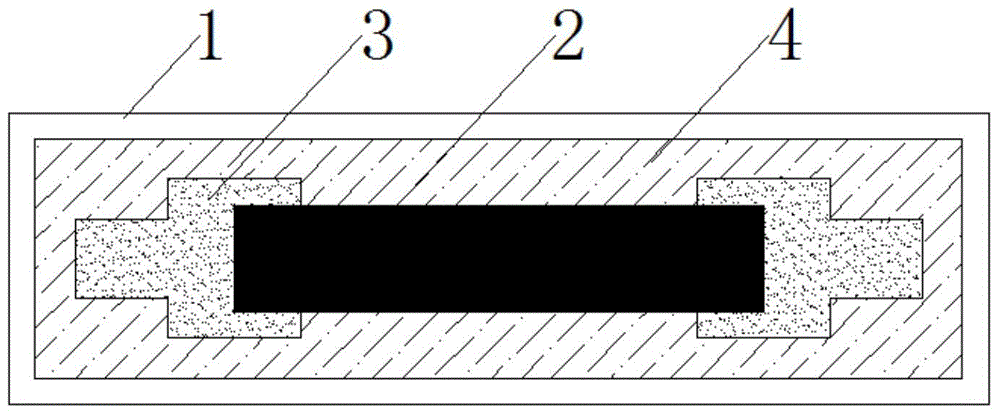
[0023] Embodiment 1: as figure 1 As shown, a modulus matching strain test sensing element of the present invention is in the shape of a strip, which includes a thin plate 1 in the lower layer, a sensitive film 2 in the middle layer, electrodes 3 and an insulating protective film 4 in the upper layer. The object of the strain test is concrete structure, and the epoxy resin sheet with smaller elastic modulus is selected as the lower sheet 1, the thickness of the sheet 1 is 0.3mm, the length is 50mm, and the width is 10mm. The sensitive film 2 of the middle layer is made of epoxy resin as the matrix and conductive carbon black as the filling material, which is prepared into a conductive polymer composite material, and then printed on the thin plate 1; before printing, the upper surface of the thin plate 1 is wiped clean with a solvent to ensure that the printing Effect. The electrodes 3 of the middle layer are printed on the thin plate 1 using commercially available printable co...
Embodiment 2
[0024] Embodiment 2: as figure 1 As shown, a modulus matching strain test sensing element of the present invention is in the shape of a strip, which includes a thin plate 1 in the lower layer, a sensitive film 2 in the middle layer, electrodes 3 and an insulating protective film 4 in the upper layer. The object to be subjected to strain testing is a high-pressure polyethylene plastic PE structure. A low-pressure polyethylene PE sheet with a smaller elastic modulus is selected as the lower sheet 1. The thickness of the sheet 1 is 0.3mm, the length is 50mm, and the width is 10mm. The sensitive film 2 of the middle layer is made of phenoxy resin as a matrix and conductive carbon nanotubes as a filling material, and is prepared into a conductive polymer composite material, which is then printed on the thin plate 1; before printing, the upper surface of the thin plate 1 is cleaned with a solvent to ensure D. The electrodes 3 of the middle layer are printed on the thin plate 1 usin...
Embodiment 3
[0025] Embodiment 3: as figure 1 As shown, a modulus matching strain test sensing element of the present invention is in the shape of a strip, which includes a thin plate 1 in the lower layer, a sensitive film 2 in the middle layer, electrodes 3 and an insulating protective film 4 in the upper layer. The object of the strain test is the soil structure. A silicon rubber sheet with a smaller elastic modulus is selected as the lower sheet 1. The thickness of the sheet 1 is 0.1mm, the length is 50mm, and the width is 10mm. The sensitive film 2 of the middle layer is made of silicone rubber as a matrix and conductive carbon black as a filling material, and is prepared into a conductive polymer composite material, and then printed on the thin plate 1; before printing, the upper surface of the thin plate 1 is cleaned with a solvent to ensure the printing effect . The electrodes 3 of the middle layer are printed on the thin plate 1 using commercially available printable conductive si...
PUM
| Property | Measurement | Unit |
|---|---|---|
| Thickness | aaaaa | aaaaa |
| Thickness | aaaaa | aaaaa |
| Length | aaaaa | aaaaa |
Abstract
Description
Claims
Application Information
 - Generate Ideas
- Intellectual Property
- Life Sciences
- Materials
- Tech Scout
- Unparalleled Data Quality
- Higher Quality Content
- 60% Fewer Hallucinations
Browse by: Latest US Patents, China's latest patents, Technical Efficacy Thesaurus, Application Domain, Technology Topic, Popular Technical Reports.
© 2025 PatSnap. All rights reserved.Legal|Privacy policy|Modern Slavery Act Transparency Statement|Sitemap|About US| Contact US: help@patsnap.com

