A method of nanoimprinting to prepare a flexible and transparent surface-enhanced Raman scattering substrate
A surface-enhanced Raman and nanoimprinting technology, which is applied in the direction of surface reaction electrolytic coatings, coatings, electrolytic coatings, etc., can solve the problems of not being suitable for mass production, harmful gas emissions, and the need for special personnel to operate, etc., to achieve excellent Reproducible, easy handling, uniform structure results
- Summary
- Abstract
- Description
- Claims
- Application Information
AI Technical Summary
Problems solved by technology
Method used
Image
Examples
Embodiment 1
[0029] A method for preparing a flexible transparent surface-enhanced Raman scattering substrate by nanoimprinting includes the following steps:
[0030] 1. Preparation of nano-imprint template:
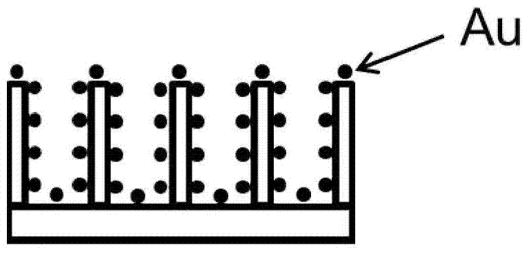
[0031] Pure aluminum (above 99.99%) is put into a 0.1-0.5 mol / L oxalic acid, sulfuric acid or phosphoric acid solution and a two-step electrochemical anodization method is adopted to prepare an anodic aluminum oxide template with adjustable size. The anode voltage is 20~200V, the temperature is 0~15℃, the first oxidation time is 2~5 hours; after the first anodic oxidation, it is soaked in 6wt% phosphoric acid and 1.8wt% chromic acid mixed solution for 4~8h, The temperature is 50~60℃; then, the second step of oxidation is carried out under the same conditions as the first anodic oxidation, and the oxidation time is 1~10 minutes; after the two steps of oxidation, 5wt% phosphoric acid solution is used to expand the holes at a temperature of 60℃ 30~180s, and then repeatedly rinse with deioni...
Embodiment 2
[0039] 1. The preparation of the nanoimprint template is the same as the first step of Example 1.
[0040] 2. Deposition of precious metal nanoparticles is the same as the second step of Example 1.
[0041] 3. Imprinting:
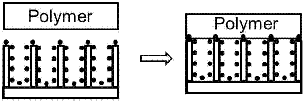
[0042] 1) Place an IPS plastic sheet (manufactured by OBDUCAT) and a porous alumina template deposited with gold nanoparticles on the sample stage, and then heat to 155°C after vacuuming; 2) Gradually pressurize to 40Bar and keep it for 5-10min 3) Reduce the pressure to 10~30Bar and keep it for 10~60S; 4) Increase the pressure to 40Bar again and keep it for 5~10min; 5) After cooling, reduce pressure. Such as image 3 Shown.
[0043] 4. Demoulding:
[0044] After the imprinting is completed, use sodium hydroxide (or potassium hydroxide) solution to remove the porous alumina and aluminum base, and then repeatedly rinse and dry with deionized water to obtain a flexible and transparent surface-reinforced Raman substrate, such as Figure 4 Shown.
PUM
 Abstract
Description
Claims
Application Information
 - R&D
- Intellectual Property
- Life Sciences
- Materials
- Tech Scout
- Unparalleled Data Quality
- Higher Quality Content
- 60% Fewer Hallucinations
Browse by: Latest US Patents, China's latest patents, Technical Efficacy Thesaurus, Application Domain, Technology Topic, Popular Technical Reports.
© 2025 PatSnap. All rights reserved.Legal|Privacy policy|Modern Slavery Act Transparency Statement|Sitemap|About US| Contact US: help@patsnap.com


