A Wide Range Variable Gain Amplifier
A gain amplifier and amplifier technology, used in differential amplifiers, DC-coupled DC amplifiers, gain control, etc., can solve the problems of poor performance stability, small signal dynamic range, and low linearity of open-loop variable gain amplifiers
- Summary
- Abstract
- Description
- Claims
- Application Information
AI Technical Summary
Problems solved by technology
Method used
Image
Examples
Embodiment 1
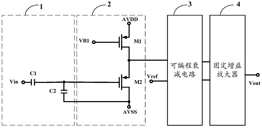
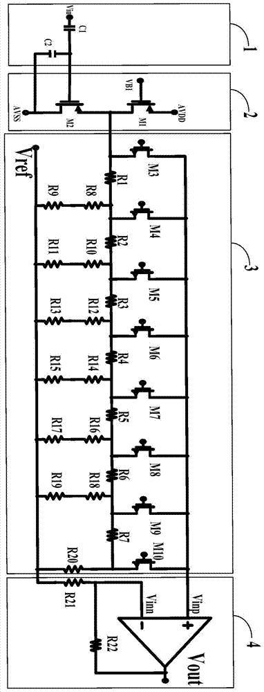
[0044] Such as figure 1 What is shown is a schematic structural diagram of a wide-range variable gain amplifier provided by an embodiment of the present invention, including: a pre-circuit 1, a source follower circuit 2, a programmable attenuation circuit 3, and a fixed gain amplifier 4;
[0045] The first end of the front end circuit 1 is connected to the signal input terminal Vin, the second end of the front end circuit 1 is connected to the ground port AVSS, and the third end of the front end circuit 1 is connected to the first input end of the source follower circuit 2. The second input terminal of the source follower circuit 2 is connected to the first bias voltage VB1; the output terminal of the source follower circuit 2 is connected to the first input terminal of the programmable attenuation circuit 3; the second input terminal of the programmable attenuation circuit 3 Connected to the reference voltage Vref; the output terminal of the programmable attenuation circuit 3 is ...
Embodiment 2
[0049] See figure 1 On the basis of the first embodiment, the front-end circuit 1 includes a first capacitor C1 and a second capacitor C2. The first terminal of the first capacitor C1 is connected to the signal input terminal Vin, and the second terminal of the first capacitor C1 is connected to the signal input terminal Vin. The first terminal of the second capacitor C2 is connected to the first input terminal of the source follower circuit 2; the second terminal of the second capacitor C2 is connected to the ground port AVSS.
[0050] It should be noted that the first capacitor C1 prevents direct current signals and low frequency signals from affecting the input signal, and the second capacitor C2 has a noise reduction function.
Embodiment 3
[0052] See figure 1 On the basis of the second embodiment, the source follower circuit 2 includes: a first transistor M1 and a second transistor M2. Both the first transistor M1 and the second transistor M2 are P-channel field effect transistors, wherein,
[0053] The gate of the first transistor M1 is connected to the first bias voltage VB1, the source of the first transistor M1 is connected to the power supply AVDD, the drain of the first transistor M1 is respectively connected to the source of the second transistor M2 and the programmable attenuation circuit 3 The first input terminal of the second transistor M2 is connected to the ground terminal AVSS.
[0054] It should be noted that the source follower circuit 2 has a boosting function. When the input signal voltage is too low, the input signal is boosted to meet higher circuit requirements.
PUM
 Abstract
Description
Claims
Application Information
 - R&D
- Intellectual Property
- Life Sciences
- Materials
- Tech Scout
- Unparalleled Data Quality
- Higher Quality Content
- 60% Fewer Hallucinations
Browse by: Latest US Patents, China's latest patents, Technical Efficacy Thesaurus, Application Domain, Technology Topic, Popular Technical Reports.
© 2025 PatSnap. All rights reserved.Legal|Privacy policy|Modern Slavery Act Transparency Statement|Sitemap|About US| Contact US: help@patsnap.com


