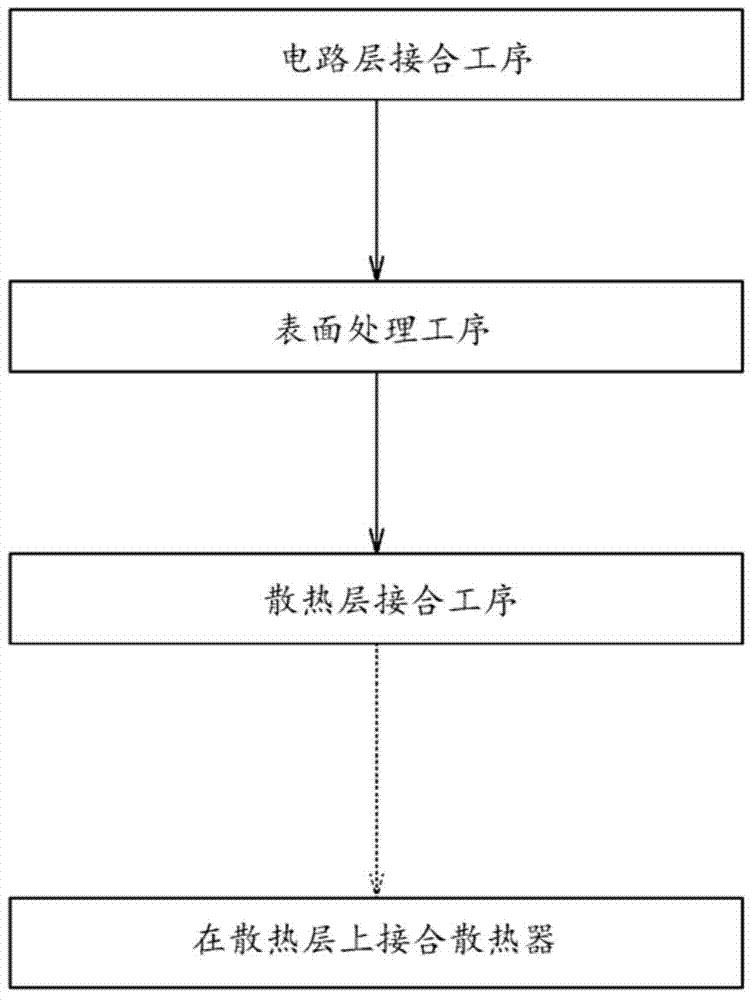
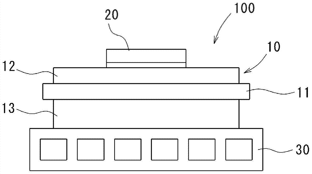
Method for producing substrate for power modules
A technology of a power module and a manufacturing method, which is applied in the field of manufacturing substrates for power modules, can solve problems such as increased peeling of the bonding interface between a ceramic substrate and a heat dissipation layer, and achieve the effects of high bonding reliability and corrosion inhibition
- Summary
- Abstract
- Description
- Claims
- Application Information
AI Technical Summary
Problems solved by technology
Method used
Image

Examples
Example Embodiment
[0043] Example
[0044] In order to confirm the effect of the manufacturing method by the power module board|substrate demonstrated above, the experiment was performed.
[0045] First, ceramic substrates made of AlN of 30 mm square were prepared as samples a to g. Among them, the ceramic substrates of the samples b to g were subjected to heat treatment at 860° C. for 30 minutes, assuming that they were bonded by active metal brazing. Then, among the samples b to g to which the heat treatment was applied, the samples c to g were surface-treated with an acid as described below. The thickness of each oxide film in the samples a to g after each treatment was measured.
[0046] a: No heat treatment
[0047] b: heat treatment only
[0048] c: After heat treatment, immersion in 18% by mass hydrochloric acid for 2.5 minutes
[0049] d: After heat treatment, immersed in 18% by mass hydrochloric acid for 5 minutes
[0050] e: After heat treatment, immersion in 18% by mass hydrochl...
PUM
 Abstract
Description
Claims
Application Information
 - Generate Ideas
- Intellectual Property
- Life Sciences
- Materials
- Tech Scout
- Unparalleled Data Quality
- Higher Quality Content
- 60% Fewer Hallucinations
Browse by: Latest US Patents, China's latest patents, Technical Efficacy Thesaurus, Application Domain, Technology Topic, Popular Technical Reports.
© 2025 PatSnap. All rights reserved.Legal|Privacy policy|Modern Slavery Act Transparency Statement|Sitemap|About US| Contact US: help@patsnap.com