Printed circuit board and method for manufacturing printed circuit board

A technology for printed circuit boards and sub-boards, which is applied in the directions of printed circuit components, electrical connection formation of printed components, electrical connection of printed components, etc., and can solve problems affecting the electrical performance of printed circuit boards and damage to the anti-corrosion layer

Active Publication Date: 2017-11-24
HONOR DEVICE CO LTD
View PDF5 Cites 0 Cited by
  • Summary
  • Abstract
  • Description
  • Claims
  • Application Information

AI Technical Summary

Problems solved by technology

[0004] However, with the above-mentioned processing, in order to avoid liquid medicine remaining in the holes, it is necessary to protect all other holes on the first sub-circuit board except the through hole C. The most commonly used method is to use an anti-corrosion layer to protect all other holes mentioned above hole, and then perform electroplating on the through hole, or process the circuit patterning on the surface of the printed circuit board. Make the other holes around the through hole C flow into the liquid medicine, thus affecting the electrical performance of the final printed circuit board

Method used


Image

  • Printed circuit board and method for manufacturing printed circuit board
  • Printed circuit board and method for manufacturing printed circuit board
  • Printed circuit board and method for manufacturing printed circuit board

Examples


Embodiment Construction

[0060] The following will clearly and completely describe the technical solutions in the embodiments of the present invention with reference to the accompanying drawings in the embodiments of the present invention. Obviously, the described embodiments are only some, not all, embodiments of the present invention. Based on the embodiments of the present invention, all other embodiments obtained by persons of ordinary skill in the art without creative efforts fall within the protection scope of the present invention.

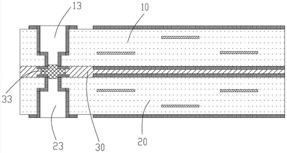
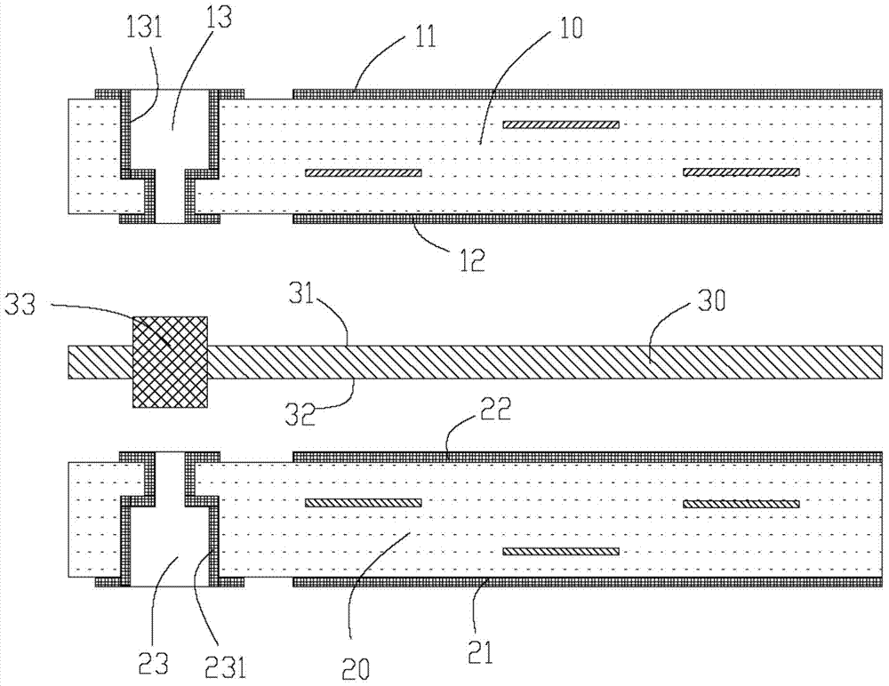
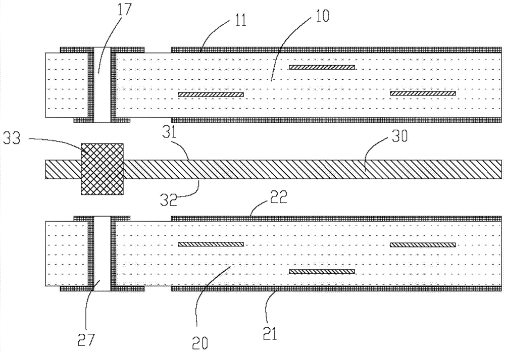
[0061] see figure 1 and figure 2 , an embodiment of the present invention provides a printed circuit board, and the printed circuit board 100 includes a plurality of sub-boards. The multiple sub-boards include a first sub-board 10 and a second sub-board 20 and a first dielectric layer 30 between the first sub-board 10 and the second sub-board 20 . Wherein, the first sub-board 10 is located on the outermost layer of the plurality of stacked sub-boards, and the fi...


PUM


Abstract

The invention provides a printed circuit board. The printed circuit board comprises a plurality of sub board bodies. The sub board bodies comprise the first sub board body and the second sub board body. A first medium layer is arranged between the first sub board body and the second sub board body. The first sub board body is located on the outmost side of the printed circuit board. The first surface of the first medium layer is in press fit with the pressing face of the first sub board body, and the second surface is in press fit with the second sub board body. The part, protruding out of the first surface, of a first guide connection column covers hole openings of via holes of the first sub board body. The part, protruding out of the second surface, of the first guide connection column covers hole openings of via holes of the second sub board body so that a conductive metal layer of the via holes of the first sub board body can be electrically connected with a conductive meal layer of the via holes of the second sub board body in a breakover mode through the first guide connection column. The invention provides a printed circuit board manufacturing method.

Description

technical field [0001] The invention relates to the field of electronic devices, in particular to a printed circuit board and a method for manufacturing the printed circuit board. Background technique [0002] With the development of science and technology, people have higher and higher requirements for the integration of integrated circuit boards. Ordinary single-sided crimping cannot meet the needs of system capacity. Double-sided crimping blind hole design is adopted, that is, two sub-boards are superimposed to form a mother board. Board structure, which can realize double-sided crimping and expand the capacity of the backplane. In addition, the demand for high-speed performance makes the density of the crimping connectors smaller and smaller, and the pitch of the crimping blind holes on the corresponding printed circuit board is getting smaller and smaller. [0003] In the prior art, when a printed circuit board is formed by laminating three or more sub-boards, and a bl...

Claims


Application Information

Patent Timeline
Patent Type & Authority Patents(China)
IPC IPC(8): H05K1/11H05K3/40
Inventor 刘山当高峰杨永星
Owner HONOR DEVICE CO LTD
Why Eureka
Try Eureka