Light emitting diode packaging method

A technology of light-emitting diodes and packaging methods, which is applied in the direction of electrical components, circuits, semiconductor devices, etc., can solve the problems affecting the accuracy of packaging components and the difficulty of ensuring accuracy, so as to avoid time consumption and accuracy errors, simplify the packaging structure, reduce cost effect

Inactive Publication Date: 2015-07-01
ZHANJING TECH SHENZHEN +1
View PDF3 Cites 4 Cited by
  • Summary
  • Abstract
  • Description
  • Claims
  • Application Information

AI Technical Summary

Problems solved by technology

[0004] In this manufacturing method, the step of "inserting light-emitting diode grains into the reflective cup structure" needs to align the light-emitting diode grains with the conductive copper plate. Due to the limitation of the accuracy of the alignment mechanical equipment, small-sized light-emitting diodes It is difficult to ensure the accuracy of the packaging position of the die in the reflective cup structure, which affects the accuracy of the entire packaging component

Method used


Image

  • Light emitting diode packaging method
  • Light emitting diode packaging method
  • Light emitting diode packaging method

Examples


Embodiment Construction

[0013] The LED packaging method provided by the embodiment of the present invention includes the following steps.

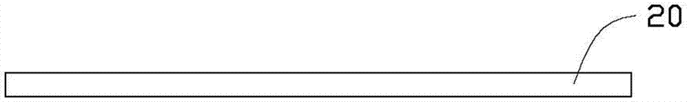
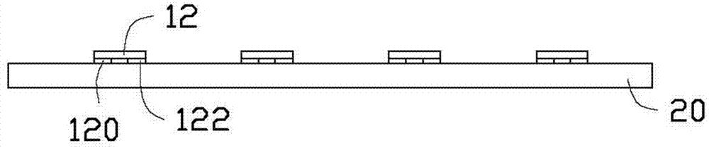
[0014] first step, see figure 1 and figure 2 , providing a viscous and elastic film layer 20 and disposing a plurality of LED chips 12 on the film layer 20 , the two electrodes 120 , 122 of each LED chip 12 are attached to the film layer 20 .

[0015] In this embodiment, the film layer 20 is a UV film or a polyimide (Polyimide) film, and the plurality of LED chips 12 are disposed on the film layer 20 by flip-chip.

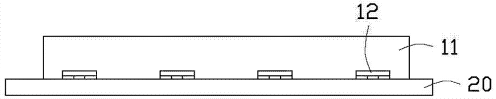
[0016] The second step, see image 3 , forming an encapsulation layer 11 on the film layer 20 and making the encapsulation layer 11 cover the plurality of LED dies 12 .

[0017] Phosphor powder can be mixed in the encapsulation layer 11 , so as to emit light with a wavelength different from that of the light-emitting diode grain 12 under light excitation of the light-emitting diode grain 12 , so as to obtain light of a desired color through light...


PUM


Abstract

A light emitting diode packaging method comprises the steps of 1 providing a first viscous film layer and arranging multiple light emitting diode crystal grains on the first film layer; 2 forming a packaging layer on the first film layer and enabling the packaging layer to cover the multiple light emitting diode crystal grains; 3 cutting the packaging layer between every two light emitting diode crystal grains so as to form a cutting way, wherein a light emitting diode unit is formed between every two adjacent cutting ways; 4 providing a second viscous film layer, transferring the light emitting diode units to the second film layer; 5 forming multiple connected optical lenses on the second film layer, wherein each optical lens corresponds to one light emitting diode unit and wraps the light emitting diode unit; 6 removing the film layer; 7 cutting the multiple connected optical lenses so as to obtain multiple light emitting diode packaging bodies.

Description

technical field [0001] The invention relates to a semiconductor light emitting device packaging method, in particular to a light emitting diode packaging method. Background technique [0002] Compared with traditional light sources, light emitting diodes (Light Emitting Diode, LED) have the advantages of light weight, small size, low pollution, long life, etc. As a new type of light source, it has been increasingly used in In various fields, such as street lights, traffic lights, signal lights, spotlights and decorative lights. [0003] The existing LED packaging structure usually includes a lead frame with a metal conductive line and a reflective cup structure, a light-emitting diode chip arranged in the reflective cup structure of the lead frame and electrically connected to the metal conductive line, and filled in the reflective cup structure And cover the packaging body of the light emitting diode chip. When making this kind of light-emitting diode packaging structure,...

Claims


Application Information

Patent Timeline
Patent Type & Authority Applications(China)
IPC IPC(8): H01L33/48H01L33/54
CPCH01L33/48H01L33/005H01L33/54
Inventor 张书修陈滨全陈隆欣曾文良
Owner ZHANJING TECH SHENZHEN
Why Eureka
Try Eureka