Processing chamber and semiconductor processing equipment

A process chamber and reaction chamber technology, which is applied in semiconductor/solid-state device manufacturing, metal material coating process, ion implantation plating, etc. Small space, reduced manufacturing cost, compact overall structure

Active Publication Date: 2015-07-01
BEIJING NAURA MICROELECTRONICS EQUIP CO LTD
View PDF7 Cites 22 Cited by
  • Summary
  • Abstract
  • Description
  • Claims
  • Application Information

AI Technical Summary

Problems solved by technology

[0006] Second, since multiple process chambers are independent of each other and arranged radially around the transfer chamber, this arrangement takes up a large space, especially when the number of process chambers is large, so that Increased overall volume of PVD equipment

Method used


Image

  • Processing chamber and semiconductor processing equipment
  • Processing chamber and semiconductor processing equipment
  • Processing chamber and semiconductor processing equipment

Examples


Embodiment 1

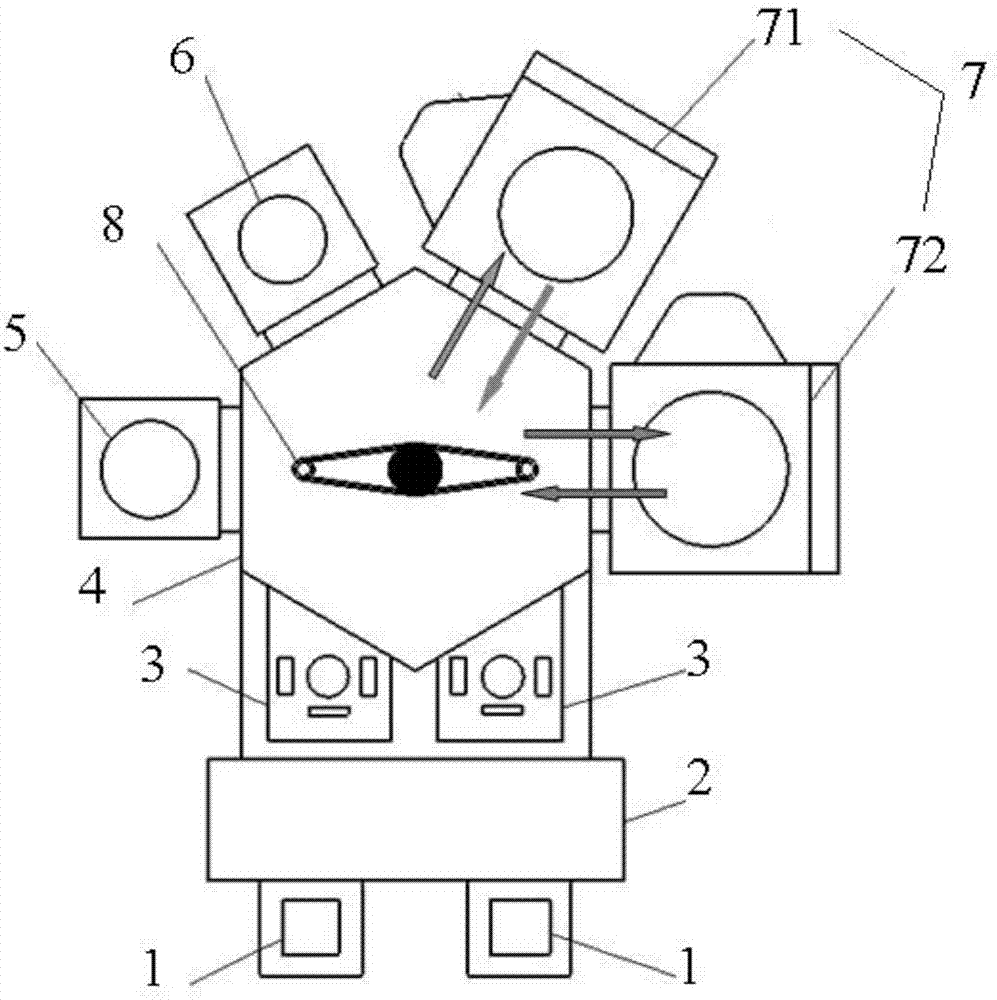
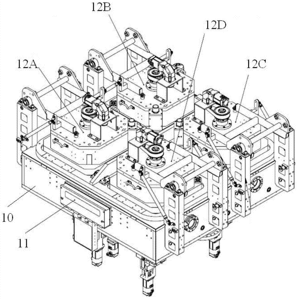
[0051] Please also refer to Figures 2A-2D , the process chamber 10 provided in this embodiment includes four reaction chambers, four sets of air intake systems and wafer transfer devices that are independent of each other. Wherein, the four reaction chambers are respectively: reaction chamber 12A, reaction chamber 12B, reaction chamber 12C and reaction chamber 12D, such as Figure 2A As shown, four reaction chambers are arranged inside the process chamber 10, and are evenly distributed along its circumference, and each reaction chamber constitutes an independent process environment, and utilizes four sets of air intake systems (not shown) one By correspondingly delivering process gases to the four reaction chambers and using the above-mentioned transport function of the wafer transport device, a single process chamber can simultaneously perform more than two processes.

[0052] In this embodiment, the structure of the wafer transfer device is as follows: it includes a rotati...

Embodiment 2

[0080] Compared with the first embodiment above, this embodiment differs only in that the structure of the wafer transfer device is different. Since other structures and functions of the process chamber provided in this embodiment have been described in detail in Embodiment 1 above, details will not be repeated here. In the following, only the structure of the wafer transfer device provided by this embodiment will be described in detail.

[0081] specifically, Figure 4A A perspective view of the internal structure of the process chamber provided for Embodiment 2 of the present invention. Figure 4B A top view of the internal structure of the process chamber provided by Embodiment 2 of the present invention. Please also refer to Figure 4A and Figure 4B , the wafer transfer device includes a manipulator 31 , a lifting base 13 and a thimble device 15 . Wherein, the number of lifting bases 13 corresponds to the number of reaction chambers, and the structure and function of...


PUM


Abstract

Provided in the present invention are a process chamber and a semiconductor processing apparatus. The process chamber comprises at least two reaction compartments, at least two sets of mutually independent air intake systems, and a chip transfer apparatus. The at least two reaction compartments are arranged within the process chamber and are distributed evenly in the circumferential direction thereof, and each reaction chamber constitutes therein an independent process environment. The air intake systems deliver in a one-to-one correspondence a process gas to the reaction compartments. The chip transfer apparatus is used for transferring chips into the reaction compartments. The process chamber and the semiconductor processing apparatus provided in the present invention allow for two or more processes to be carried out simultaneously in a single process chamber, thus not only is the process chamber structurally compact and small in footprint, but also obviated is the need to redesign the structure of a transfer chamber, thus allowing for reduced costs for manufacturing the apparatus.

Description

technical field [0001] The invention relates to the field of semiconductor equipment manufacturing, in particular to a process chamber and semiconductor processing equipment. Background technique [0002] The basic principle of physical vapor deposition (Physical Vapor Deposition, PVD) is: under vacuum conditions, the metal, metal alloy or compound is evaporated and deposited on the surface of the substrate to form a thin film with special functions. The main methods of physical vapor deposition are: vacuum evaporation, plasma sputtering coating, arc plasma coating, ion coating and molecular beam epitaxy. Among them, plasma sputtering coating is currently the most representative and widely used physical vapor deposition technology. When using plasma sputtering technology to deposit (coat) a semiconductor wafer, the process chamber used is usually a vacuum environment, and process gas is supplied to the process chamber and excited to form plasma, which bombards the target, ...

Claims


Application Information

Patent Timeline
Patent Type & Authority Applications(China)
IPC IPC(8): H01L21/67H01L21/677
CPCC23C14/56H01L21/67C23C14/22H01L21/67207H01L21/6719H01L21/67161H01L21/67739
Inventor 吕峰张风港赵梦欣丁培军李冬冬文莉辉
Owner BEIJING NAURA MICROELECTRONICS EQUIP CO LTD
Why Eureka
Try Eureka