
Process method of glass substrate

A glass substrate and process method technology, applied in the field of microelectronics, can solve the problems of low etching selection and unsatisfactory etching depth, etc., and achieve the effect of improving the etching selection ratio

Active Publication Date: 2016-12-07
BEIJING NAURA MICROELECTRONICS EQUIP CO LTD
View PDF6 Cites 0 Cited by
  • Summary
  • Abstract
  • Description
  • Claims
  • Application Information

AI Technical Summary

Problems solved by technology

[0008] It can be seen from the above Table 1 that although the above single-step etching method has a relatively high etching rate, the etching selection is relatively low (the maximum etching selection ratio that can be achieved is about 30:1), so it cannot meet the requirements for Processes requiring high etch depth

Method used


Image

  • Process method of glass substrate
  • Process method of glass substrate
  • Process method of glass substrate

Examples


Embodiment Construction

[0043] In order to enable those skilled in the art to better understand the technical solution of the present invention, the process method of the glass substrate provided by the present invention will be described in detail below with reference to the accompanying drawings.

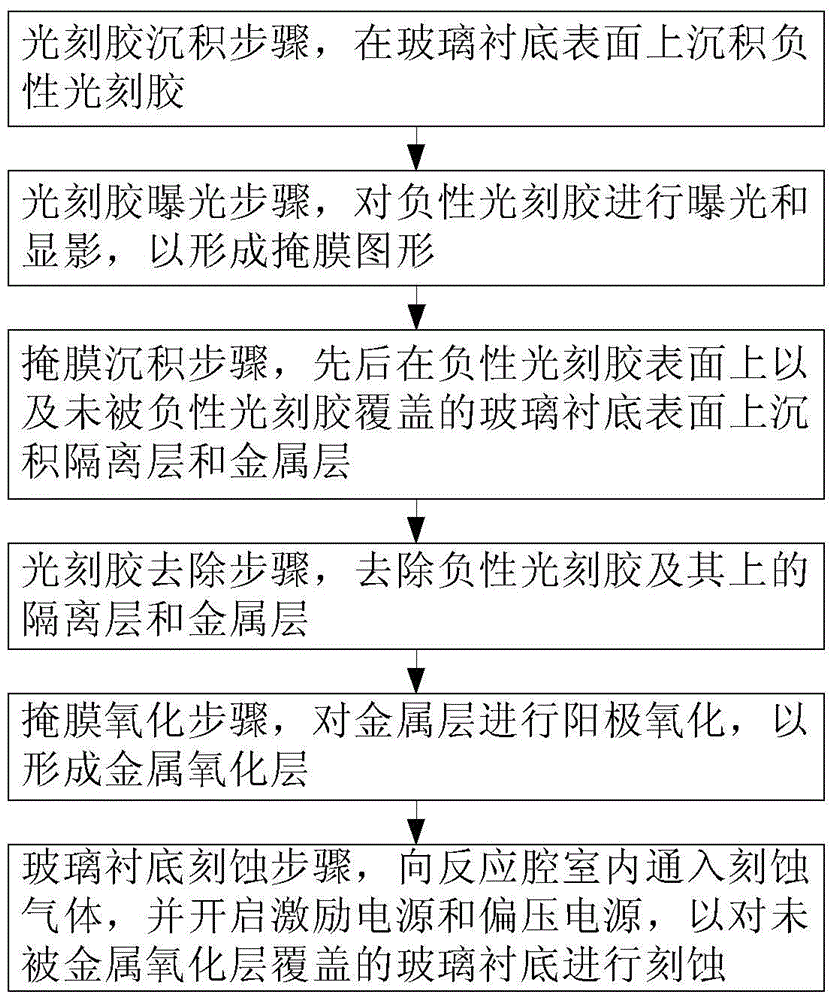
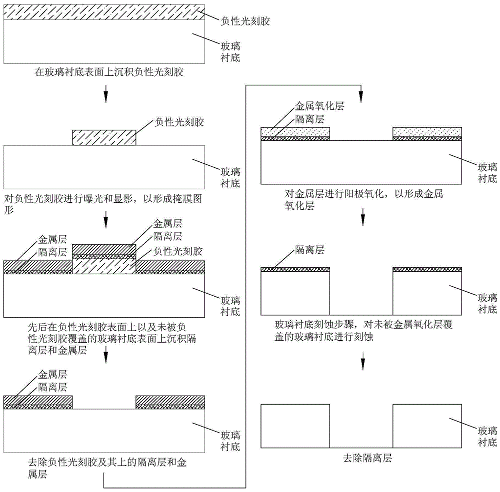
[0044] figure 1 It is a block flow diagram of a glass substrate processing method provided by the present invention. figure 2 It is a schematic diagram of the etching process of a glass substrate processing method provided by the present invention. Please also refer to figure 1 and figure 2 , the method includes the following steps:

[0045] In the photoresist deposition step, a negative photoresist is deposited on the surface of the glass substrate by magnetron sputtering, evaporation coating or chemical vapor deposition.

[0046] In the photoresist exposure step, the negative photoresist is exposed and developed to form a mask pattern, that is, the negative photoresist is used to define the patte...


PUM

PropertyMeasurementUnit
thicknessaaaaaaaaaa
thicknessaaaaaaaaaa
thicknessaaaaaaaaaa

Abstract

The invention provides a technological method for a glass substrate. The method includes: a photoresist deposition step: depositing negative photoresist on a glass substrate surface; a photoresist exposure step: exposing and developing negative photoresist to form a mask pattern; a mask deposition step: depositing an isolation layer and a metal layer on the negative photoresist surface and the glass substrate surface not covered by the negative photoresist in order, wherein the isolation layer is prepared from an anti-anodic oxidation material, and the metal layer is prepared from a bivalent or trivalent metal material; a photoresist removal step: removing the negative photoresist and the isolation layer and the metal layer thereon; and a mask oxidation step: carrying out anodic oxidation on the metal layer to form the metal oxide layer. The technological method for the glass substrate provided by the invention can improve the etching selection ratio of the glass substrate to the mask.

Description

technical field [0001] The invention relates to the technical field of microelectronics, in particular to a process method of a glass substrate. Background technique [0002] At present, in the manufacturing process of MEMS devices, glass (silicon dioxide) is used as the substrate material, because glass substrates have higher insulation than silicon substrates, so that MEMS devices can be applied in high Fields that require high insulation such as voltage and high power. In the various processes of manufacturing MEMS devices, the etching process is one of the important processes. Its main working process is: depositing a mask on the glass substrate and etching a pattern on the mask; etching the surface of the glass substrate The area not covered by the mask on the glass substrate is used to etch the required pattern on the surface of the glass substrate. [0003] In practical applications, the etching process of glass substrates usually requires a large etching depth. Th...

Claims


Application Information

Patent Timeline
Patent Type & Authority Patents(China)
IPC IPC(8): B81C1/00
Inventor 张宇
Owner BEIJING NAURA MICROELECTRONICS EQUIP CO LTD
Learn More