An optical multiplexer and an optical emitting device
An optical multiplexer and optical component technology, applied in the field of optical communication, can solve the problems of optical path imbalance, complex assembly process, and high difficulty in AWG fabrication
- Summary
- Abstract
- Description
- Claims
- Application Information
AI Technical Summary
Problems solved by technology
Method used
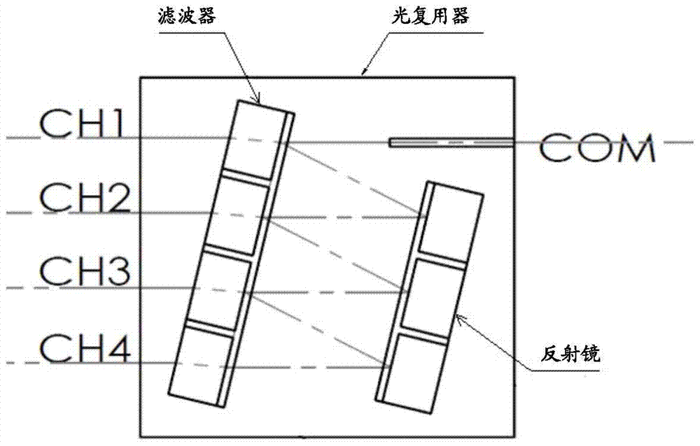
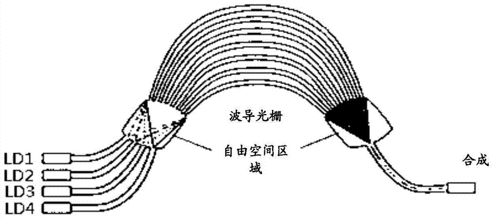
Image

Examples
Embodiment 1
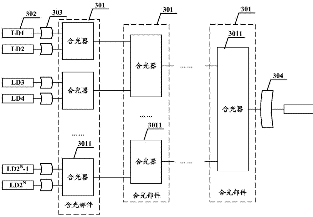
[0070] Take 4 beams of light as an example to illustrate. In this embodiment, firstly, 2 PBC light combiners are used as the first-level light combining components to combine 4 beams of light into 2 beams, and then a beam splitting prism light combiner is used as the The second-stage light-combining component further combines the two beams of light into one beam of light and outputs it.
[0071] Such as Figure 6 As shown, after the light emitted by LD1 is collimated by the collimating lens (Lens), and then rotated 90 degrees by the half-wave plate whose optical axis is at an angle of 45 degrees to the polarization direction of the incident light, its polarization direction is exactly the same as that of the light emitted by LD2 The directions are perpendicular to each other, and after turning the light path through the reflector, it can combine with the light emitted by LD2 through PBC1 to form a beam of light, and then incident on a beam splitting prism placed at an angle of...
Embodiment 2
[0073] Take 4 beams of light as an example to illustrate. In this embodiment, firstly, 2 beam splitting prism light combiners are used as the first-level light combining components to combine 4 beams of light into 2 beams, and then a PBC light combiner is used as the The second-stage light-combining component further combines the two beams of light into one beam of light and outputs it.
[0074] Such as Figure 7 As shown, the light emitted by LD1 is collimated by the collimating lens, then passes through the reflector to turn the light path, and is reflected by 50% of the energy by the 3dB dichroic prism, and then combined with the light emitted by LD2 and transmitted by 50% of the energy by the 3dB dichroic prism Light; similarly, the light emitted by LD4 is collimated by the collimating lens, then passes through the mirror to turn the light path, and is reflected by 50% of the energy by the 3dB beam splitting prism, and synthesized with the light emitted by LD3 and transmit...
PUM
 Abstract
Description
Claims
Application Information
 - R&D
- Intellectual Property
- Life Sciences
- Materials
- Tech Scout
- Unparalleled Data Quality
- Higher Quality Content
- 60% Fewer Hallucinations
Browse by: Latest US Patents, China's latest patents, Technical Efficacy Thesaurus, Application Domain, Technology Topic, Popular Technical Reports.
© 2025 PatSnap. All rights reserved.Legal|Privacy policy|Modern Slavery Act Transparency Statement|Sitemap|About US| Contact US: help@patsnap.com