Method for forming semiconductor device
A semiconductor and device technology, applied in the field of semiconductor device formation, can solve the problem that the performance of semiconductor devices needs to be improved, and achieve the effects of improving carrier mobility, good quality and superior performance
- Summary
- Abstract
- Description
- Claims
- Application Information
AI Technical Summary
Problems solved by technology
Method used
Image

Examples
Embodiment Construction
[0024] As mentioned in the background, the performance of semiconductor devices formed by using the prior art still needs to be improved.
[0025] After research, it is found that the performance of semiconductor devices in the prior art is mainly restricted by carrier mobility. Specifically, the carrier mobility is closely related to the performance of the material of the channel region and components around the channel region, as well as the quality of formation, carrier scattering in the channel region, and interface state density.
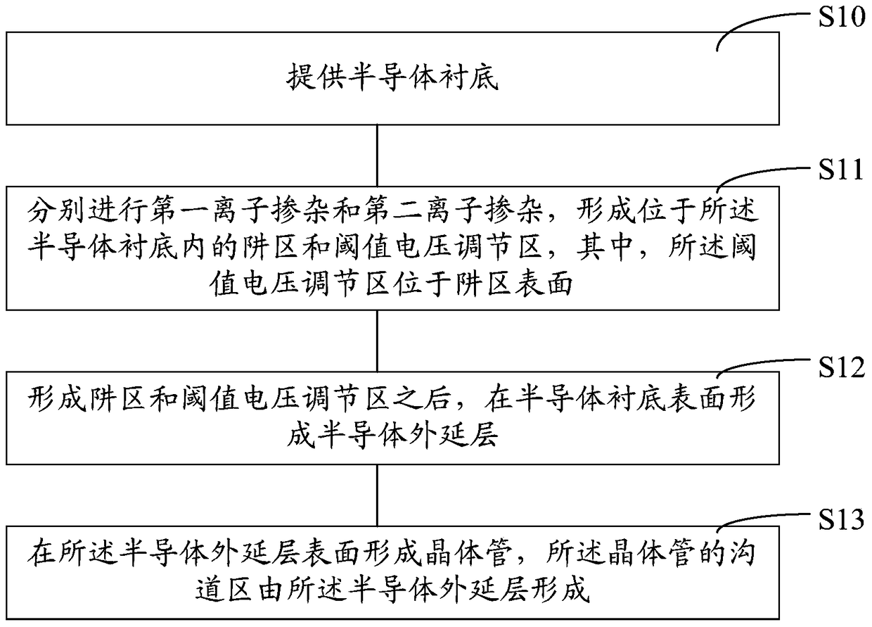
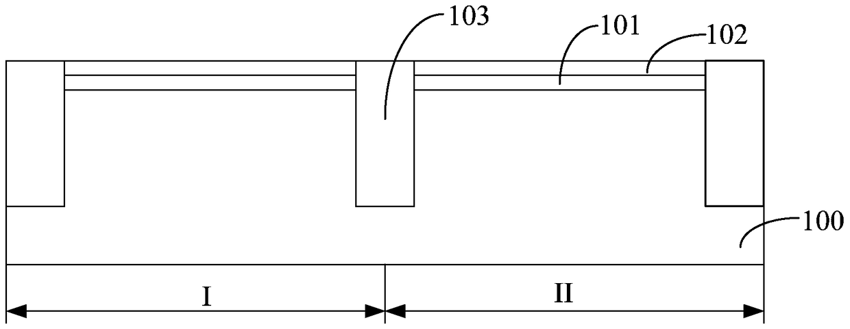
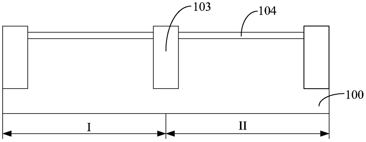
[0026] After further research, it is found that in the prior art, when forming a semiconductor device, a SiGe epitaxial layer is first formed on the surface of the semiconductor substrate, and then a transistor is formed, and the channel region of the transistor is formed by the SiGe epitaxial layer. However, in the process of forming a transistor, steps such as ion implantation to form a well region and a threshold voltage adjustment region ar...
PUM
 Abstract
Description
Claims
Application Information
 - R&D
- Intellectual Property
- Life Sciences
- Materials
- Tech Scout
- Unparalleled Data Quality
- Higher Quality Content
- 60% Fewer Hallucinations
Browse by: Latest US Patents, China's latest patents, Technical Efficacy Thesaurus, Application Domain, Technology Topic, Popular Technical Reports.
© 2025 PatSnap. All rights reserved.Legal|Privacy policy|Modern Slavery Act Transparency Statement|Sitemap|About US| Contact US: help@patsnap.com