An ultra-broadband absorber based on cascaded metamaterials
A cascade structure and metamaterial technology, applied in the direction of instruments, instrument parts, shielding, etc., can solve the problems of narrow absorption wavelength range, low absorption rate, small incident angle, etc., and achieve easy processing and preparation, lower absorption frequency, The effect of broadening the absorption bandwidth
- Summary
- Abstract
- Description
- Claims
- Application Information
AI Technical Summary
Problems solved by technology
Method used
Image
Examples
specific Embodiment approach 1
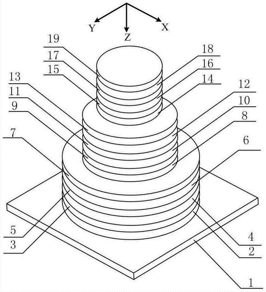
[0014] Specific implementation mode one: as figure 1 As shown, an ultra-broadband absorber based on cascaded metamaterials in this embodiment consists of a metal plate substrate 1, a first dielectric layer 2, a first metal layer 3, a second dielectric layer 4, and a second metal layer 5 , the third dielectric layer 6, the third metal layer 7, the fourth dielectric layer 8, the fourth metal layer 9, the fifth dielectric layer 10, the fifth metal layer 11, the sixth dielectric layer 12, the sixth metal layer 13, the The seventh dielectric layer 14, the seventh metal layer 15, the eighth dielectric layer 16, the eighth metal layer 17, the ninth dielectric layer 18 and the ninth metal layer 19; the metal plate substrate 1 is horizontally placed on the bottom layer, in the The center position of the metal plate substrate 1 is arranged in parallel from bottom to top with a first dielectric layer 2, a first metal layer 3, a second dielectric layer 4, a second metal layer 5, a third d...
specific Embodiment approach 2
[0020]Embodiment 2: The difference between this embodiment and Embodiment 1 is: the metal plate substrate 1, the first metal layer 3, the second metal layer 5, the third metal layer 7, the fourth metal layer 9, The materials of the fifth metal layer 11, the sixth metal layer 13, the seventh metal layer 15, the eighth metal layer 17 and the ninth metal layer 19 are all gold, aluminum or copper, and the thickness is 20nm; the metal plate substrate 1 is a square metal plate with a side length of 400 nm. This setting makes the transmittance T(ω) 0, which meets the actual needs. Other steps and parameters are the same as in the first embodiment.
[0021] The thickness of the square metal plate in this embodiment is greater than the skin depth of the incident electromagnetic wave.
[0022] In this embodiment, the formula A(w)=1-R(ω)-T(ω) is used to calculate the absorptivity of the metamaterial absorber, wherein R(ω) is the reflectivity, and T(ω) is the transmittance. In order to ...
specific Embodiment approach 3
[0023] Embodiment 3: This embodiment differs from Embodiment 1 or Embodiment 2 in that: the first dielectric layer 2, the first metal layer 3, the second dielectric layer 4, the second metal layer 5, and the third dielectric layer 6 and the diameter of the bottom surface of the third metal layer 7 is 175 nm. Other steps and parameters are the same as those in Embodiment 1 or 2.
PUM
 Abstract
Description
Claims
Application Information
 - R&D
- Intellectual Property
- Life Sciences
- Materials
- Tech Scout
- Unparalleled Data Quality
- Higher Quality Content
- 60% Fewer Hallucinations
Browse by: Latest US Patents, China's latest patents, Technical Efficacy Thesaurus, Application Domain, Technology Topic, Popular Technical Reports.
© 2025 PatSnap. All rights reserved.Legal|Privacy policy|Modern Slavery Act Transparency Statement|Sitemap|About US| Contact US: help@patsnap.com


