
Photoelectric information conversion element and application thereof

An information conversion and component technology, applied in the field of wide-spectrum response, can solve the problem that the conversion component does not have continuous photoconductivity, and achieve the effect of reducing resistance and increasing the degree of energy level bending.

Active Publication Date: 2015-06-10
NINGBO INST OF MATERIALS TECH & ENG CHINESE ACADEMY OF SCI
View PDF8 Cites 6 Cited by
  • Summary
  • Abstract
  • Description
  • Claims
  • Application Information

AI Technical Summary

Problems solved by technology

The current photoelectric signal conversion usually uses the photoconductive properties of semiconductor materials, that is, light can change the resistance of the conversion element, and when the light is stopped, the resistance of the element returns to the initial state, that is, the conversion element has no continuous photoconductivity.

Method used


Image

  • Photoelectric information conversion element and application thereof
  • Photoelectric information conversion element and application thereof
  • Photoelectric information conversion element and application thereof

Examples


Embodiment 1

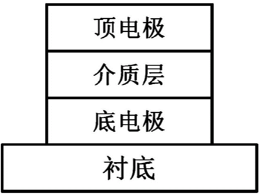
[0044] In this embodiment, the structure of the photoelectric information conversion element is as follows figure 1 As shown, including substrate, bottom electrode, dielectric layer and top electrode. The bottom electrode is located on the substrate, and the dielectric layer is located between the bottom electrode and the top electrode.

[0045] In this embodiment, the substrate is made of Si substrate; the bottom electrode is made of metal aluminum; the dielectric layer is made of cerium oxide film, preferably 20-30nm thick; the top electrode is made of ITO film, the thickness of which is 100um.

[0046] In this embodiment, the photoelectric information conversion element is prepared by coating method, which includes the following steps:

[0047] (1) The Si substrate was ultrasonically cleaned with acetone, ethanol, and deionized water for 10 minutes. After taking it out, it was blown dry with nitrogen, and then placed in the vacuum chamber of the electron beam evaporation s...

Embodiment 2

[0075] In this embodiment, the structure of the photoelectric information conversion element is basically the same as that in Embodiment 1, except that the dielectric layer uses a zinc oxide film instead of the cerium oxide film in Embodiment 1.

[0076] In this embodiment, the preparation method of the photoelectric information conversion element is basically the same as that in Embodiment 1, except that in step (2), a zinc oxide film is deposited by sputtering.

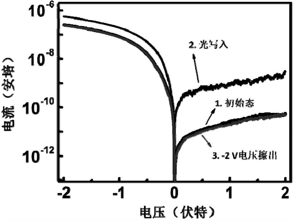
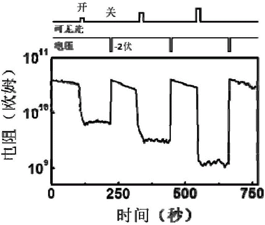
[0077] The photoelectric conversion properties of the photoelectric information conversion element were characterized using a Keithley 4200 semiconductor parameter measuring instrument, and the characterization method was the same as that in Example 1. The results show that the element has continuous photoconductive properties, that is, the light can change the resistance of the element, and the resistance can be restored to the initial state by using the reverse voltage. Therefore, the element is a wide-spectrum re...


PUM


Abstract

The invention provides a photoelectric information conversion element, comprising a top electrode, a medium layer and a bottom electrode, wherein the medium layer and at least one of the bottom electrode and the top electrode form a Schottky junction. The element has a wide spectrum effect to light; when light irradiates the element, the characteristics of the Schottky junction are regulated by photogenerated holes in a node region, so that the resistance of the element is changed continuously; moreover, the resistance of the element is regulated polymorphically by controlling the strength and / or wavelength of the irradiating light; in addition, electrons can be injected to the interface of the Schottky junction by applying certain voltage, so that the resistance of the element recovers to the initial state. Therefore, the element has wide spectrum response and sustainable photoconduction and can be applied to many fields such as a multifunctional optical detector, an intelligent photosensor, an optical signal operational unit, an optical information decoding (or encoding) device and a nonvolatile memory.

Description

technical field [0001] The invention relates to the technical field of photoelectric information conversion, in particular to a wide-spectrum response, sustainable photoelectric information conversion element and its application. Background technique [0002] Photoelectric information conversion, that is, converting optical signals into electrical signals, is one of the important components of optical interconnection chips. The performance of the photoelectric information conversion element determines its role in the optical interconnection chip. Current photoelectric signal conversion usually uses the photoconductive properties of semiconductor materials, that is, light can change the resistance of the conversion element, and when the light is stopped, the resistance of the element returns to the initial state, that is, the conversion element does not have continuous photoconductivity. If the performance of photoconductivity can be changed essentially through the selection...

Claims


Application Information

Patent Timeline
Patent Type & Authority Applications(China)
IPC IPC(8): H01L31/0224H01L31/04H01L31/07H01L31/02H01L31/08
CPCY02E10/50H01L31/0224H01L31/02H01L31/022408H01L31/04H01L31/07H01L31/08
Inventor 李润伟檀洪伟刘钢
Owner NINGBO INST OF MATERIALS TECH & ENG CHINESE ACADEMY OF SCI
Learn More