Display panel and display device

A display panel and display device technology, which is applied to optics, instruments, electrical components, etc., can solve the problems of display panel display abnormal distortion, driving signal instability, and overlapping area increase, so as to achieve difficult display abnormal distortion, stable driving signal, The effect of reducing the overlapping area

Active Publication Date: 2017-10-31
INNOLUX CORP
View PDF6 Cites 0 Cited by
  • Summary
  • Abstract
  • Description
  • Claims
  • Application Information

AI Technical Summary

Problems solved by technology

This type of display panel mainly uses oxide semiconductor, because it needs to protect the oxide semiconductor layer with an etch stop layer (ESL), so the area of ​​source S1 and drain S2 must be increased to be effective. driving, and then the overlapping area of ​​the gate G and the source S1 and drain S2 increases, resulting in an increase in the load capacitance
Also, according to the formula for calculating panel power consumption P=f*C*V 2 It can be seen that the increase of the capacitance value (C) will increase its power consumption (P), which will easily cause the driving signal to be unstable, making the display panel prone to abnormal display distortion.

Method used


Image

  • Display panel and display device
  • Display panel and display device
  • Display panel and display device

Examples


Embodiment Construction

[0081] A display panel and a display device according to preferred embodiments of the present invention will be described below with reference to related drawings, wherein the same elements will be described with the same reference symbols.

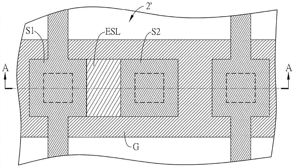
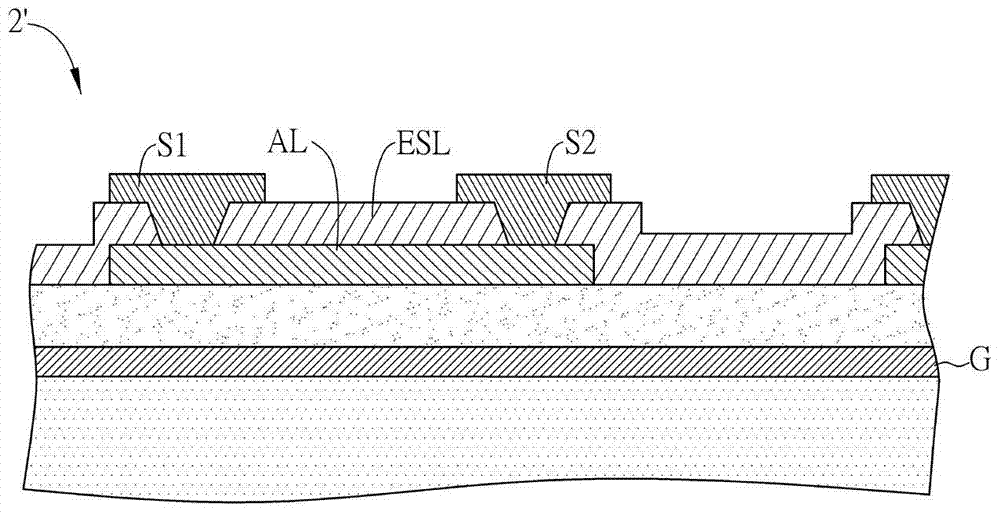
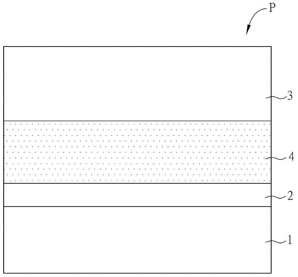
[0082] figure 2 For a schematic cross-sectional view of a display panel according to an embodiment of the present invention, please refer to figure 2 , the display panel P of this embodiment includes a first substrate 1 , a plurality of pixels 2 , a second substrate 3 , and a display medium 4 . In detail, the first substrate 1 and the second substrate 3 are, for example, transparent substrates (such as glass substrates or polymer substrates), and one of the first substrate 1 and the second substrate 3 may be provided with a color filter layer (not shown). drawn). A plurality of pixels 2 are arranged on the first substrate 1 . The second substrate 3 is disposed on the first substrate 1 , wherein a plurality of pixels 2 are located bet...


PUM

PropertyMeasurementUnit
capacitanceaaaaaaaaaa
power consumptionaaaaaaaaaa

Abstract

The invention provides a display panel and a display device. The display panel includes a first substrate and a plurality of pixels. The pixels are arranged on the first substrate and include a gate line area, an active layer, an etching stop layer, a first source / drain layer and a second source / drain layer. The gate line area is arranged on the first substrate and has a first area and a second area, the first area has a first part and the second area has a second part, and the first part and the second part respectively have a first A width and a second width, the first width is greater than the second width. The active layer is disposed on the gate line area, has a channel area, and the channel area is disposed on the first part. The etch stop layer, the first source / drain layer and the second source / drain layer are arranged on the active layer, and the active layer between the first source / drain layer and the second source / drain layer is a channel region . Through the present invention, the load capacitance can be reduced, so as to achieve the effect of reducing the power signal and stabilizing the driving signal.

Description

technical field [0001] The invention relates to liquid crystal display technology, in particular to a display panel and a display device. Background technique [0002] Common display panels or display devices include liquid crystal displays or organic light emitting diode displays. Regardless of any display panel or display device, an amorphous silicon (a-Si) thin film transistor or a low temperature polysilicon (Low Temperature Polycrystalline, LTPS) thin film transistor is required as a switching element for driving each pixel. In recent years, many studies have pointed out that oxide semiconductor thin film transistors have higher carrier mobility than amorphous silicon thin film transistors, and oxide semiconductor thin film transistors have higher mobility than low-temperature polysilicon thin film transistors. , it has better threshold voltage uniformity. Therefore, some display panels or display devices currently use oxide semiconductors as host materials. [0003]...

Claims


Application Information

Patent Timeline
Patent Type & Authority Patents(China)
IPC IPC(8): G02F1/1362G02F1/1368H01L27/12H01L29/423H01L23/50
Inventor 蔡嘉豪
Owner INNOLUX CORP
Why Eureka
Try Eureka