


Quick Research
Generate reliable direction feasibility study reports for your R&D in just a few steps.

Technical Q&A
Discover and master advanced knowledge NOW. Basics, ideas, possibilities, all at once.

Find Solutions
As an expert in R&D theories, this can generate solutions to your technical problems instantly.

Evaluate Feasibility
Analyze your overall solution with one click, know your potential R&D risks in advance.

Monitor Landscape
Get weekly tech updates, stay abreast of the latest tech innovations and key insights.
Organic light-emitting device and production method thereof
An electroluminescent device and electroluminescent technology, which are applied in the manufacturing of organic semiconductor devices, electric solid-state devices, semiconductor/solid-state devices, etc., can solve the problems of poor water and oxygen isolation ability, reduced luminous efficiency, and low electron transfer rate.
- Summary
- Abstract
- Description
- Claims
- Application Information
AI Technical Summary
Problems solved by technology
Method used
Image

Examples
preparation example Construction
[0032] The method for preparing the above-mentioned organic electroluminescent device specifically includes the following steps:
[0033] 1. Rinse the glass with distilled water and ethanol, and soak it in isopropanol overnight.
[0034] 2. Prepare a conductive anode film on the glass cleaned in the above steps to obtain an anode conductive substrate, and then vapor-deposit sequentially on the anode conductive substrate to prepare a hole injection layer, a hole transport layer, a light-emitting layer, and an electron transport layer.
[0035] 3. Next, an electron injection layer is prepared on the above electron transport layer, and the electron injection layer is composed of a passivation layer, a rubidium compound doped layer and a rhenium compound layer. First prepare the passivation layer by electron beam, the thickness is 1-10nm, and the energy density of electron beam evaporation is 10-100W / cm 2 .
[0036] Then electron beams are used to prepare the rubidium compound d...
Embodiment 1
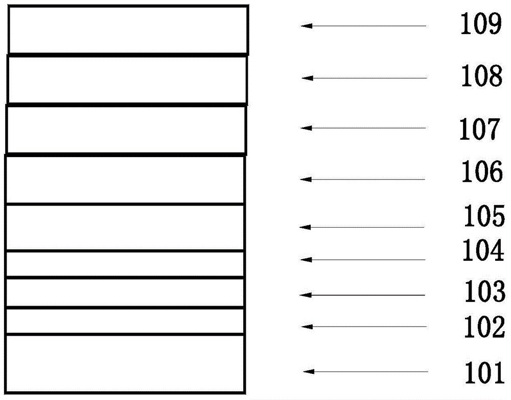
[0050] Such as figure 1 As shown, the organic electroluminescent device in this embodiment is a layered structure, and each layer is in turn:
[0051] Anode conductive substrate 101 of glass / IZO, MoO 3 The hole injection layer 102 of the material, the hole transport layer 103 of the TAPC material, the light emitting layer 104 of the ADN material, the electron transport layer 105 of the TPBI material, Al 2 o 3 Material passivation layer 106, Rb 2 CO 3 :SiO2 2 Rubidium compound doped layer 107, ReO 2 The rhenium compound layer 108 made of Ag material and the cathode layer 109 made of Ag material. The passivation layer 106, the rubidium compound doped layer 107 and the rhenium compound layer 108 form an electron injection layer. (wherein the slash " / " indicates a layered structure, and the colon ":" indicates mutual doping).
[0052] The above-mentioned organic electroluminescent device is prepared according to the following steps in sequence:
[0053] 1. Rinse the glass...
Embodiment 2
[0066] The layered structure of the organic electroluminescent device of the following examples 2-4 is basically the same as that of the example 1, so no illustration will be given here.
[0067] The organic electroluminescent device in this embodiment is a layered structure, and each layer is sequentially:
[0068] Anode conductive substrate of glass / IZO, MoO 3 Hole injection layer made of TAPC material, hole transport layer made of TAPC material, light emitting layer made of ADN material, electron transport layer made of TPBI material, SiO 2 passivation layer made of RbCl:NiO rubidium compound doped layer, ReO 3 The rhenium compound layer of material and the cathode layer of Ag material. The passivation layer, the rubidium compound doped layer and the rhenium compound layer constitute the electron injection layer. (wherein the slash " / " indicates a layered structure, and the colon ":" indicates mutual doping).
[0069] The above-mentioned organic electroluminescent devic...
PUM
 Abstract
Description
Claims
Application Information
 - R&D Engineer
- R&D Manager
- IP Professional
- Industry Leading Data Capabilities
- Powerful AI technology
- Patent DNA Extraction
Browse by: Latest US Patents, China's latest patents, Technical Efficacy Thesaurus, Application Domain, Technology Topic, Popular Technical Reports.
© 2024 PatSnap. All rights reserved.Legal|Privacy policy|Modern Slavery Act Transparency Statement|Sitemap|About US| Contact US: help@patsnap.com