Selective area growing method for III-nitride micro graphic structure and structure

A technology of selective area growth and pattern structure, applied in semiconductor devices, electrical components, circuits, etc., can solve the problems of poor uniformity, poor repeatability and high cost of micro pattern structure, and achieve flexible and controllable mask pattern shape and pattern size change. Large-scale, low-cost effects

Inactive Publication Date: 2015-05-20
PEKING UNIV
View PDF5 Cites 8 Cited by
  • Summary
  • Abstract
  • Description
  • Claims
  • Application Information

AI Technical Summary

Problems solved by technology

[0006] Among the above two types of existing methods, the thin film materials produced by the former have the advantages of good uniformity and good controllability, but the process is complicated and the cost is high, and it is still difficult to obtain a microscopic pattern structure with a characteristic size below 100nm on a large scale.
Although the latter has a relatively simple process and does not need to prepare a mask, the resulting microscopic pattern structure has poor uniformity, poor controllability, and poor repeatability.

Method used


Image

  • Selective area growing method for III-nitride micro graphic structure and structure
  • Selective area growing method for III-nitride micro graphic structure and structure
  • Selective area growing method for III-nitride micro graphic structure and structure

Examples


Embodiment 1

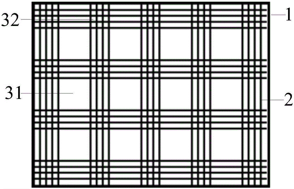
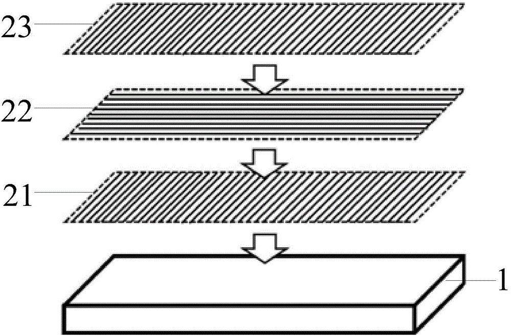
[0043] In this embodiment, a c-plane sapphire substrate is used as the substrate, and three layers of carbon nanotube films are laid on the substrate as a carbon nanotube mask to prepare a GaN double-sized micron hexagonal prism microscopic pattern structure. Such as figure 2 As shown, three layers of carbon nanotube arrays 21-23 are respectively laid on the substrate 1 as a carbon nanotube mask, the first layer 21 is perpendicular to the second layer 22, and the third layer 23 is perpendicular to the second layer; each layer The carbon nanotube film includes a plurality of cluster structures arranged in parallel, the diameter of each cluster is between 2 and 4 μm, and the distance between adjacent clusters is between 2 and 4 μm. As a micron-scale growth window, the cluster The distance between the inner adjacent carbon nanotubes is 200-500nm, and serve as nanoscale growth windows to form a micron / nano compound size mask in which micron scale growth windows and nanoscale grow...

Embodiment 2

[0055] In this embodiment, the high-temperature nitriding process in embodiment one is canceled, that is, step b) in step 3) is cancelled, and the other steps are the same as in embodiment one, and a GaN double-size micron hexagonal pyramid microscopic pattern structure can be obtained, such as Figure 4 shown.

Embodiment 3

[0057] In this embodiment, the c-plane sapphire substrate is used as the substrate, and four layers of carbon nanotube films are laid on the substrate as a carbon nanotube mask to prepare a GaN double-sized micron inverted trapezoidal microscopic pattern structure.

[0058] The selective growth method of the GaN double-size micron inverted trapezoidal micro-pattern structure in this embodiment includes the following steps:

[0059] 1) Substrate 1 adopts c-plane sapphire.

[0060] 2) laying a carbon nanotube mask on the substrate 1:

[0061] On the growth substrate of the carbon nanotube array, a layer of neatly arranged and uniformly sized nanoscale iron powder is deposited by electron beam evaporation as a catalyst, and then by LPCVD method, acetylene is used as a carbon source at low pressure and high temperature to grow quasi Ordered, parallel arrays of carbon nanotubes are peeled off and laid on the growth substrate of Group III nitrides; the formed carbon nanotubes are s...


PUM

PropertyMeasurementUnit
Diameteraaaaaaaaaa
Diameteraaaaaaaaaa
Thicknessaaaaaaaaaa

Abstract

The invention discloses a selective area growing method for III-nitride micro graphic structure and a structure. A carbon nanotube array is taken as a micrometer / nanometer composite size mask; nanometer grade growing windows in bundle clusters and micrometer grade growing windows among the bundle clusters are arranged at intervals; according to the remarkable difference between the growth rates of III-nitride in the micrometer grade growing windows and the nanometer grade growing windows, an III-nitride dual-size micro graphic structure in which micro graphic structures which are the same in shapes and are different in sizes are arranged at intervals can be made on the micrometer / nanometer composite size mask. By adopting the carbon nanotube mask, the advantage of nanoheteroepitaxy can be brought into full play, the crystal quality of a micro graphic structural material is improved, and the residual stress is lowered; the nanotube has the characteristics of high thermal conductivity and high electrical conductivity, so that the heat dissipation of subsequently-manufactured micro-electron and photoelectron devices and the improvement on the electric property are facilitated.

Description

technical field [0001] The invention relates to semiconductor optoelectronic technology, in particular to a method and structure for selective growth of a group III nitride double-sized microscopic pattern structure with carbon nanotubes as a mask, precise and controllable shape and size. Background technique [0002] Group III nitrides are a class of semiconductor materials with great application prospects. In addition to conventional thin film materials, in recent years, various micron or nanoscale group III nitrides and thin film materials with such micron or nanoscale pattern structures It also exhibits superior performance and wide application possibilities. The aforementioned microstructures include one-dimensional trench structures, two-dimensional island structures, or three-dimensional columnar structures. Such thin-film materials with microscopic graphic structures can be used as graphic templates to obtain high-quality thin-film materials, and can also be directl...

Claims


Application Information

Patent Timeline
IPC IPC(8): H01L21/02H01L29/06
CPCH01L21/02H01L21/0254H01L21/027H01L29/06
Inventor 于彤军冯晓辉程玉田吴洁君贾传宇张国义
Owner PEKING UNIV
Why Eureka
Try Eureka