
Circuit board and circuit board manufacturing method

A circuit board production and circuit board technology, which is applied in the direction of printed circuit manufacturing, printed circuit, printed circuit, etc., can solve problems such as difficulty in meeting light and thin, poor return effect, and poor conductive effect, so as to prevent electromagnetic interference and reduce The effect of production cost and shortened process

Active Publication Date: 2015-04-29
AVARY HLDG (SHENZHEN) CO LTD +1
View PDF2 Cites 14 Cited by
  • Summary
  • Abstract
  • Description
  • Claims
  • Application Information

AI Technical Summary

Problems solved by technology

However, since the conductive effect of anisotropic conductive adhesive is worse than that of metal, the resistance will change when transitioning from anisotropic conductive adhesive to metal film, so when the signal is transmitted back, the return effect will also be poor
In addition, the thickness of the anisotropic conductive adhesive is relatively thick, and the thickness of the flexible circuit board with the thicker anisotropic conductive adhesive is also relatively thick, which is difficult to meet the requirements of light and thin

Method used


Image

  • Circuit board and circuit board manufacturing method
  • Circuit board and circuit board manufacturing method
  • Circuit board and circuit board manufacturing method

Examples


Embodiment Construction

[0019] The circuit board provided by the technical solution and its manufacturing method will be further described in detail below in conjunction with the accompanying drawings and embodiments.

[0020] The circuit board manufacturing method provided by the embodiment of the technical solution includes the following steps:

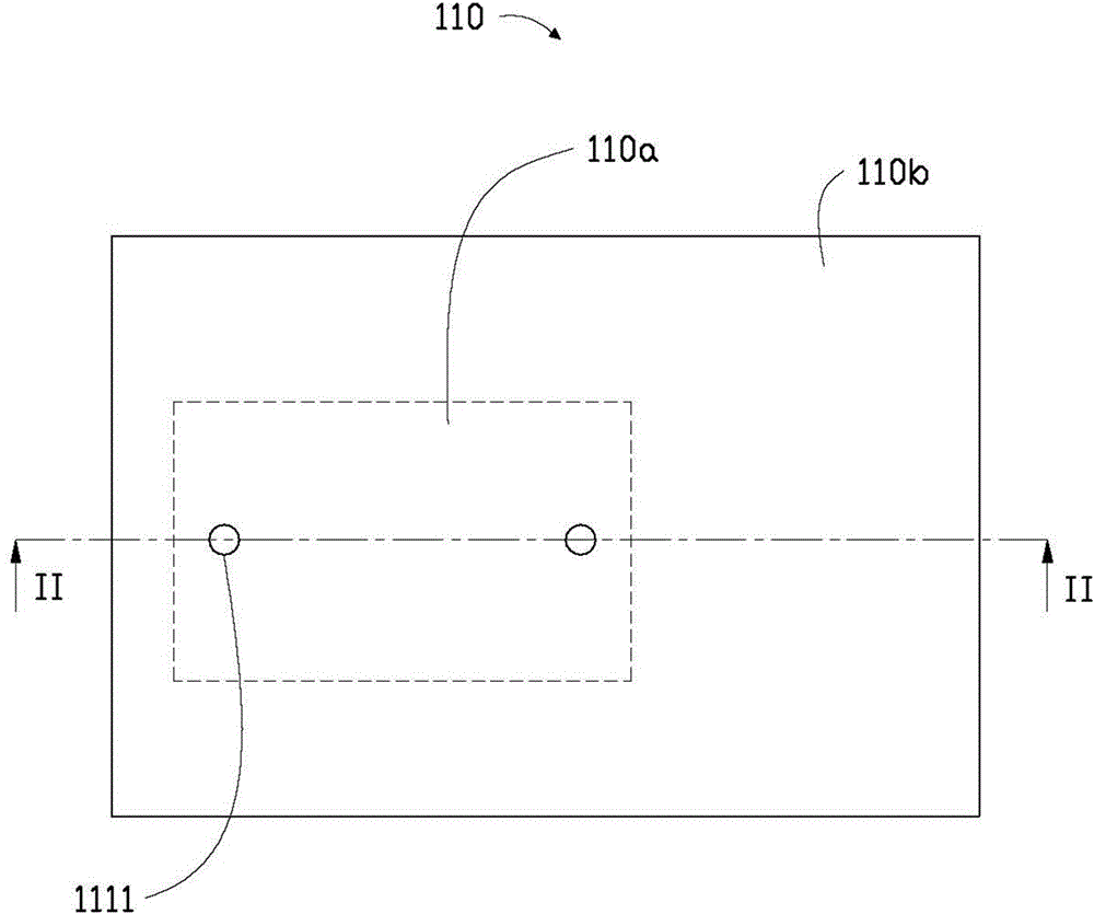
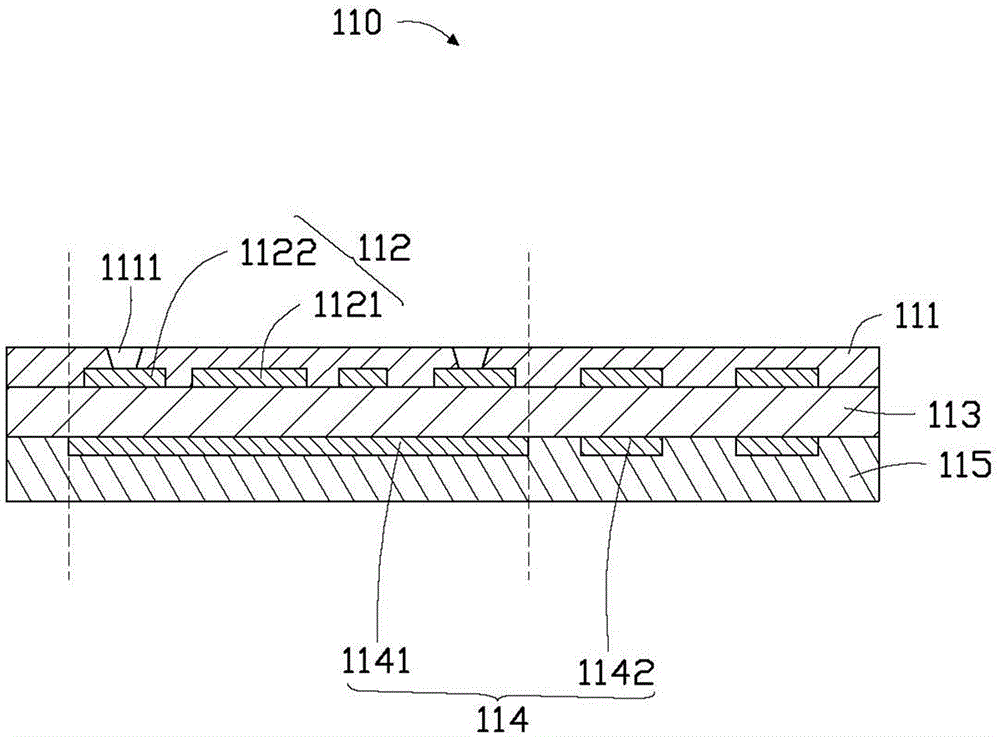
[0021] For a first step, see figure 1 and 2 , providing a circuit substrate 110 .

[0022] In this embodiment, the circuit substrate 110 is a circuit board with conductive lines formed thereon. The circuit substrate 110 includes a first insulating layer 111 , an outer conductive circuit layer 112 , a second insulating layer 113 , an inner conductive circuit layer 114 and a base layer 115 sequentially arranged from top to bottom. The circuit substrate 110 has at least one electromagnetic shielding forming region 110a and a common region 110b except the electromagnetic shielding forming region 110a, and the electromagnetic shielding forming region 110a is...


PUM


Abstract

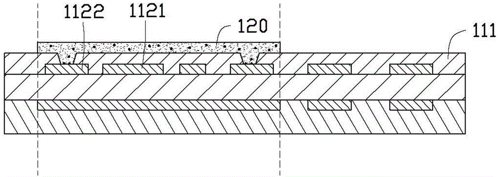
The invention relates to a circuit board which comprises a circuit substrate, an ink layer containing pure metal and an electromagnetic shielding structure, wherein the circuit substrate comprises an outer conducting circuit layer and a first insulating layer, which are in contact with each other; the outer conducting circuit layer is formed on one side of the first insulating layer and comprises a grounding circuit; open holes are formed in the first insulating layer to expose the grounding circuit; the ink layer containing the pure metal is formed on the surface, which is far from the outer conducting circuit layer, of the first insulating layer and the surface of the grounding circuit exposed out of the open holes; the grounding circuit is electrically connected with the electromagnetic shielding structure through the pure metal in the ink layer. The invention further provides a circuit board manufacturing method.

Description

technical field [0001] The invention relates to circuit board manufacturing technology, in particular to a circuit board and a circuit board manufacturing method. Background technique [0002] Due to the thinner and thinner requirements of the flexible circuit board, when the internal circuit is used as the signal line for external signal transmission, it is usually necessary to use conductive silver foil (EMI shielding film) to cover the outer layer of the flexible circuit board to prevent interference caused by external electromagnetic interference. Signal loss. [0003] Conductive silver foil usually has a four-layer structure, namely protective film, metal film, anisotropic conductive adhesive and release film. Before bonding, the release film needs to be removed, so that the anisotropic conductive adhesive and the flexible circuit board are combined with each other. However, since the conductive effect of anisotropic conductive adhesive is worse than that of metal, th...

Claims


Application Information

Patent Timeline
Patent Type & Authority Applications(China)
IPC IPC(8): H05K1/02H05K3/00
CPCH05K1/0224H05K2201/0723
Inventor 何明展胡先钦沈芾云
Owner AVARY HLDG (SHENZHEN) CO LTD
Learn More