Surface enhanced Raman scattering substrate and manufacturing method thereof
A surface-enhanced Raman and substrate technology, applied in Raman scattering, material excitation analysis, etc., can solve the problem that it is difficult to obtain the SERS surface substrate with precise control of the arraying degree, and meet the requirements of saving raw materials and energy, and surface properties Effect of low, large substrate size
- Summary
- Abstract
- Description
- Claims
- Application Information
AI Technical Summary
Problems solved by technology
Method used
Image

Examples
Embodiment 1
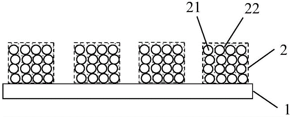
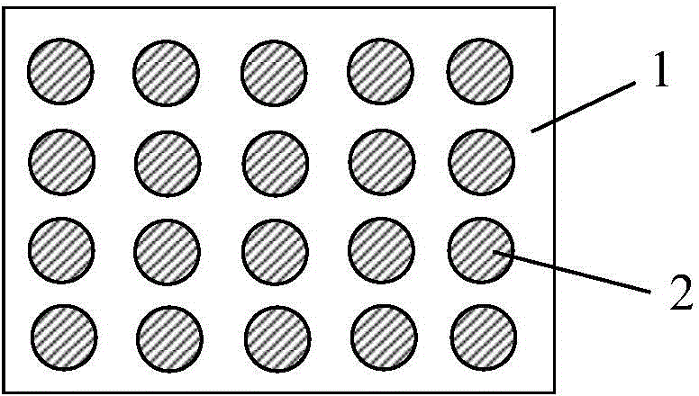
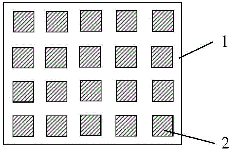
[0032] In this embodiment, the VX500 3D printer of German Voxeljet Company is used as the processing equipment. The metal nanounit array pattern on the surface of the SERS substrate is designed on the computer of the 3D printer control system. Put the substrate into the 3D printer workbench, lay a layer of Au powder with a particle size of 1nm on the substrate, and the thickness of the Au powder layer is 400nm; according to the set array pattern, the nozzle of the 3D printer is directed on the preset pattern. Add the matching adhesive of Voxeljet to the Au powder layer, and use the laser equipment attached to the 3D printer to sinter the Au powder particles adhered to the adhesive. The laser power is 200W, the sintering temperature is 1000°C, and the time is 60 seconds; the sintering is completed After that, use N 2 The gas blows off the unbonded and fixed Au powder particles to form an array of Au nanounits on the substrate, wherein the spacing of the Au nanounits is 1 μm. ...
Embodiment 2
[0034] This embodiment uses the Objet350Connex type 3D printer of Stratasys Company of the United States as the processing equipment. The metal nanounit array pattern on the surface of the SERS substrate is designed on the computer of the 3D printer control system. Put the substrate into the 3D printer workbench, lay an Ag powder layer with a particle size of 5nm on the substrate, and the thickness of the Ag powder layer is 500nm; according to the set array pattern, use the 3D printer nozzle in the direction of the preset pattern The Ag powder layer is dripped with an organic adhesive. Wherein, in terms of mass percentage, the organic adhesive contains 65% methacrylate, 22% ethylene and propylene mixture, 12% ethylene oxide, 0.8% peroxide initiator, 0.2% copper acetylacetonate ; and use the printer's UV device to quickly cure the adhesive, and then use N 2 The gas blows off the unbonded and fixed Ag powder particles, forming an Ag nanounit array structure on the substrate, w...
Embodiment 3
[0037]This embodiment uses the Objet350Connex type 3D printer of Stratasys Company of the United States as the processing equipment. The metal nanounit array pattern on the surface of the SERS substrate is designed on the computer of the 3D printer control system. Put the substrate into the 3D printer workbench, and lay a Cu powder layer with a particle size of 10nm on the substrate. The Cu powder layer is dripped with an inorganic adhesive. Wherein, in terms of mass percentage, the inorganic adhesive contains 4% sodium chloride, 6% sodium carbonate, 3% sodium bicarbonate, 7% silicic acid, 25% xylitol, and 55% water; and Use the printer's UV unit to cure the adhesive quickly, and then use the N 2 The gas blows off unbonded and fixed Cu powder particles to form a structure of Cu nanounit array on the substrate, wherein the spacing of Cu nanounits is 2 μm. Put the above-obtained Cu nano unit array substrate into a high temperature furnace at 500° C. for sintering and annealin...
PUM
| Property | Measurement | Unit |
|---|---|---|
| particle diameter | aaaaa | aaaaa |
| thickness | aaaaa | aaaaa |
| thickness | aaaaa | aaaaa |
Abstract
Description
Claims
Application Information
 - R&D
- Intellectual Property
- Life Sciences
- Materials
- Tech Scout
- Unparalleled Data Quality
- Higher Quality Content
- 60% Fewer Hallucinations
Browse by: Latest US Patents, China's latest patents, Technical Efficacy Thesaurus, Application Domain, Technology Topic, Popular Technical Reports.
© 2025 PatSnap. All rights reserved.Legal|Privacy policy|Modern Slavery Act Transparency Statement|Sitemap|About US| Contact US: help@patsnap.com