LDS electroless plating process

A technology of electroless plating and electroless nickel plating, applied in the field of electroless plating technology, can solve problems affecting the development of copper surface treatment technology, overflow plating of catalytically active products of electroless plating solution, affecting product quality and production cost, etc., to achieve the suppression of overflow plating , Solve the problem of overflow plating, solve the effect of overflow plating phenomenon

Inactive Publication Date: 2015-04-29
SHANGHAI AMPHENOL AIRWAVE COMM ELECTRONICS CO LTD
View PDF5 Cites 5 Cited by
  • Summary
  • Abstract
  • Description
  • Claims
  • Application Information

AI Technical Summary

Problems solved by technology

[0015] However, when electroless copper and nickel plating is performed on lasered plastic parts, overflow plating often occurs, which seriously affects product quality and production cost, so controlling the electroless plating overflow has become an urgent problem to be solved
In the existing electroless plating process, if palladium activation is not well controlled, it will be easily overactivated, so that palladium is also deposited on non-copper surfaces, and then nickel is also deposited, resulting in overflow plating
In addition, the stability of the electroless plating solution and others such as the temperature of electroless plating, the choice of reducing agent, the high catalytic activity, and the selection and dosage of activator in the pretreatment are likely to cause the occurrence of product overflow plating, which seriously affects The actual production and the development of copper surface treatment technology

Method used


Image

  • LDS electroless plating process
  • LDS electroless plating process
  • LDS electroless plating process

Examples


Embodiment

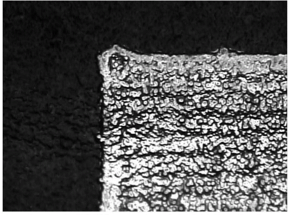
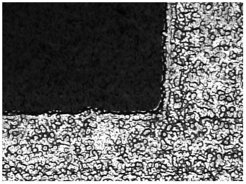
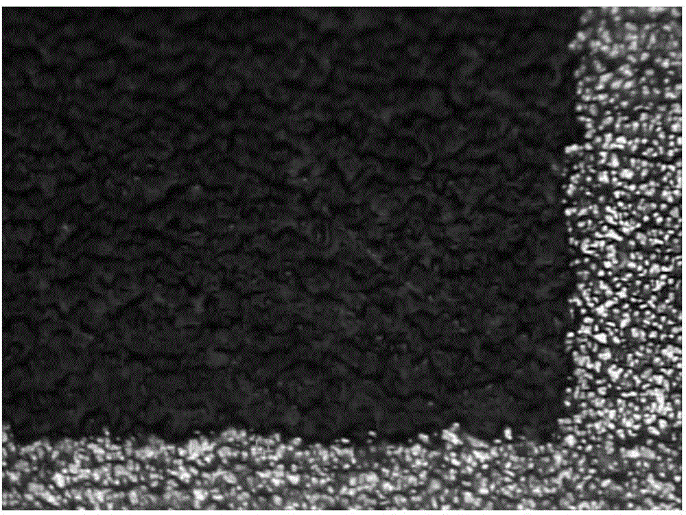
[0072] Using the above-mentioned LDS electroless plating process, the present embodiment has selected two representative mobile phone antenna products, namely: antenna A and antenna B, wherein antenna A and antenna B are made of polycarbonate (PC) and acrylonitrile - Butadiene-styrene copolymer (ABS) is mixed, and the two antenna products are semi-finished products, which are made by laser machine of LPKF company according to different antenna patterns.


PUM


Abstract

The invention discloses an LDS (Laser Direct Structuring) electroless plating process. The LDS electroless plating process comprising the following steps: firstly, performing pretreatment on an LDS product printed with a copper circuit to remove an oxide film on the surface of copper; secondly, performing nickel dipping processing on the LDS product subjected to pretreatment in nickel dipping liquid to enable metallic nickel to be deposited on the surface of copper so as to obtain a nickel catalyst layer; thirdly, performing activating treatment on the LDS product in an activation solution to active the catalytic activity of nickel dipping copper surface to electroless nickel plating; fourthly, immersing the LDS product in an electroless nickel plating bath to perform electroless nickel plating according to a conventional method. The LDS electroless plating process not only can improve an overflow plating condition, but also can reduce the raw material cost.

Description

technical field [0001] The invention relates to an electroless plating process in the LDS technology, in particular to an LDS electroless copper plating and nickel plating process. Background technique [0002] 3D-MID (Three-dimensional molded interconnect device, three-dimensional molded interconnect device) technology appeared in the 1980s and is a technology for making three-dimensional circuits. Judging from the market statistics released by foreign countries, three-dimensional circuits are currently popularized in nearly 30 industries in China. The largest market is in the field of communication (mobile phone antenna) (80%), followed by multi-chip micropackaging (9%), automotive electronics (3%), confidential products (3%), medical product industry (3%), the application prospect is very broad, and the market potential is huge. [0003] 3D-MID is to make wires and graphics with electrical functions on the special injection-molded plastic shell, so as to combine the elec...

Claims


Application Information

Patent Timeline
Patent Type & Authority Applications(China)
IPC IPC(8): C23C18/30C23C18/36C23C18/38B32B15/04
Inventor 刘阳
Owner SHANGHAI AMPHENOL AIRWAVE COMM ELECTRONICS CO LTD
Why Eureka
Try Eureka