Diamond nano needle array composite material and preparation method and application thereof
A composite material and nano-needle technology, applied in the field of diamond nano-needle array composite material and its preparation, can solve the problems of small shape factor, poor thermal conductivity, weak super-emission performance, etc., and achieve good consistency, improved stability, excellent Effects of Field Emission Characteristics
- Summary
- Abstract
- Description
- Claims
- Application Information
AI Technical Summary
Problems solved by technology
Method used
Image
Examples
preparation example Construction
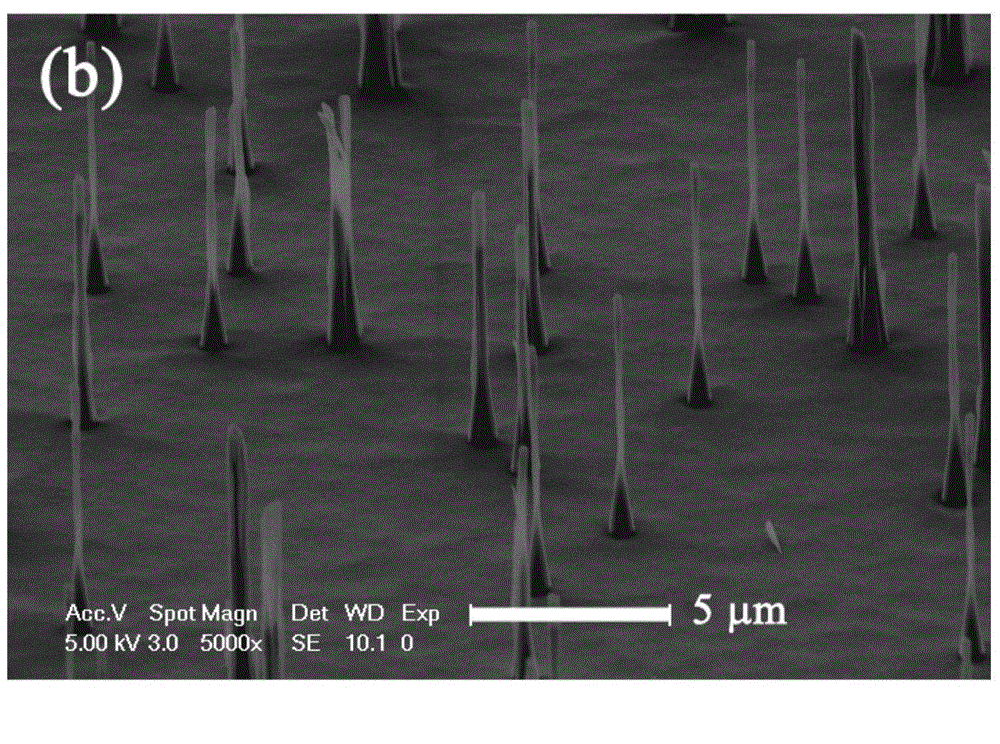
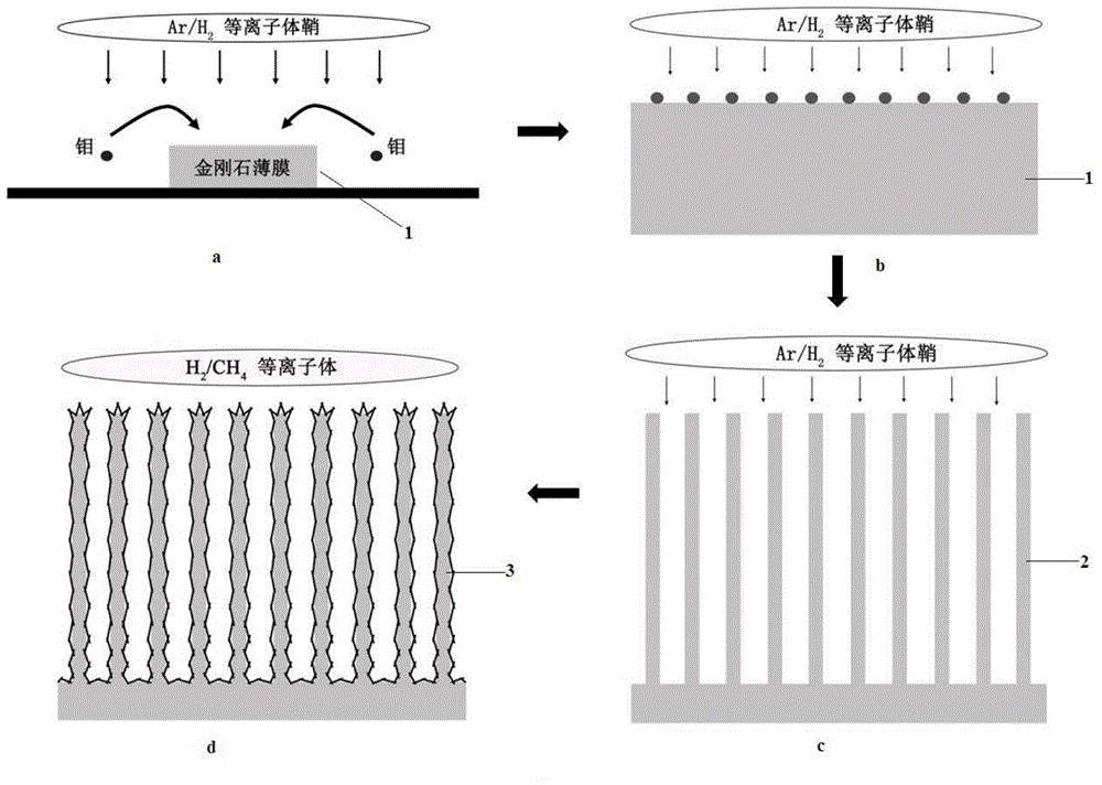
[0042] Correspondingly, on the basis of the above-mentioned diamond nanoneedle array composite material, the embodiment of the present invention also provides a preparation method of the diamond nanoneedle array composite material, the process flow of which is as follows figure 1 As shown, please refer to Figures 2 to 3 at the same time. The preparation method of the diamond nanoneedle array composite material comprises the following steps:
[0043] Step S01: Depositing a diamond film layer 1 on the surface of the substrate;
[0044] Step S02: Etching the diamond film layer 1 to form a diamond nanoneedle array 2;
[0045] Step S03: using chemical vapor deposition to grow a three-dimensional graphene layer on the surface of the diamond nanoneedles in the diamond nanoneedle array 2 to form a diamond nanoneedle array 3 with a three-dimensional graphene layer grown on the surface.
[0046] Specifically, in the above step S01, in the substrate ( figure 1 For showing) the method ...
Embodiment 1
[0065] A diamond nano needle array composite material and a preparation method thereof. The preparation method process of the diamond nanoneedle array composite material is as follows: figure 1 , which includes the following steps:
[0066] S11. Prepare a diamond film layer 1 deposited on the surface of the substrate:
[0067] A micron nitrogen-doped nanocrystalline diamond film layer was prepared on a 1 cm×1 cm, n-type (001) silicon wafer by microwave plasma CVD. Before the growth, the silicon substrate was ultrasonically treated with diamond powder for 60 minutes, and the cleaned silicon substrate was placed on a molybdenum substrate table, and placed in a CVD device, and vacuumed to 10 -5 Pa. The specific parameters of its microwave plasma CVD method growth are as follows: methane / hydrogen volume ratio: methane / nitrogen / hydrogen volume ratio: 10% / 45% / 45%, total gas flow: 200sccm, air pressure: 30Torr, microwave power: 1200W, Silicon substrate temperature: 800°, depositi...
Embodiment 2
[0073] A diamond nano needle array composite material and a preparation method thereof. Reference to the preparation method of the diamond nanoneedle array composite material figure 1 , which includes the following steps:
[0074] S21. Prepare a diamond film layer 1 deposited on the surface of the substrate:
[0075] A micron nitrogen-doped nanocrystalline diamond film layer was prepared on a 1 cm×1 cm, n-type (001) silicon wafer by microwave plasma CVD. Before the growth, the silicon substrate was ultrasonically treated with diamond powder for 60 minutes, and the cleaned silicon substrate was placed on a molybdenum substrate table, and placed in a CVD device, and vacuumed to 10 -5 Pa. The specific parameters of its microwave plasma CVD method growth are as follows: methane / hydrogen volume ratio: 10%, total gas flow rate: 200sccm, air pressure: 30Torr, microwave power: 1200W, silicon substrate temperature: 800°C, deposition time: 24 hours;
[0076] S22. Etching the diamond...
PUM
| Property | Measurement | Unit |
|---|---|---|
| diameter | aaaaa | aaaaa |
| height | aaaaa | aaaaa |
| diameter | aaaaa | aaaaa |
Abstract
Description
Claims
Application Information
 - R&D
- Intellectual Property
- Life Sciences
- Materials
- Tech Scout
- Unparalleled Data Quality
- Higher Quality Content
- 60% Fewer Hallucinations
Browse by: Latest US Patents, China's latest patents, Technical Efficacy Thesaurus, Application Domain, Technology Topic, Popular Technical Reports.
© 2025 PatSnap. All rights reserved.Legal|Privacy policy|Modern Slavery Act Transparency Statement|Sitemap|About US| Contact US: help@patsnap.com


