LED substrate structure and manufacturing method thereof
A technology of substrate structure and manufacturing method, which is applied in the direction of electrical components, circuits, semiconductor devices, etc., can solve the problems of low light output efficiency of flip-chip LED chips, improve axial luminous brightness, strong operability, and improve light output efficiency Effect
- Summary
- Abstract
- Description
- Claims
- Application Information
AI Technical Summary
Problems solved by technology
Method used
Image
Examples
Embodiment 1
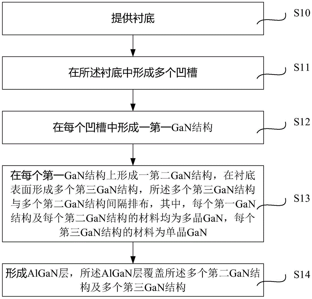
[0055] Please refer to Figure 2 to Figure 9 , which is a schematic diagram of a device structure formed in the method for manufacturing an LED substrate structure according to Embodiment 1 of the present invention.
[0056] like figure 2 As shown, a substrate 20 is provided, preferably, the substrate 20 is a sapphire substrate.
[0057] Next, a plurality of grooves are formed in the substrate 20, specifically, please refer to Figure 3 ~ Figure 5 .
[0058] First, if image 3 As shown, a mask layer 21 is formed on the substrate 20 . Preferably, the material of the mask layer 21 is at least one of silicon dioxide, silicon nitride and silicon oxynitride. In the embodiment of the present application, the mask layer 21 may be formed by an evaporation process, a sputtering process, a PECVD process, or an LPCVD process.
[0059] Next, if Figure 4 As shown, a plurality of openings 22 are formed in the mask layer 21 to expose part of the substrate 20 . Here, a part of the m...
Embodiment 2
[0072] The difference between the second embodiment and the first embodiment is that the shape of the groove is an inverted triangle, that is, the shape of the first GaN structure is an inverted triangle. Specifically, please refer to Figure 10 ~ Figure 17 , which is a schematic diagram of the device structure formed in the method for manufacturing the LED substrate structure according to the second embodiment of the present invention.
[0073] like Figure 10 As shown, a substrate 30 is provided, preferably, the substrate 30 is a sapphire substrate.
[0074] Next, a plurality of grooves are formed in the substrate 30, specifically, please refer to Figure 11 ~ Figure 13 .
[0075] First, if Figure 11 As shown, a mask layer 31 is formed on the substrate 30 . Preferably, the material of the mask layer 31 is at least one of silicon dioxide, silicon nitride and silicon oxynitride. In the embodiment of the present application, the mask layer 31 may be formed by an evaporat...
PUM
 Abstract
Description
Claims
Application Information
 - R&D Engineer
- R&D Manager
- IP Professional
- Industry Leading Data Capabilities
- Powerful AI technology
- Patent DNA Extraction
Browse by: Latest US Patents, China's latest patents, Technical Efficacy Thesaurus, Application Domain, Technology Topic, Popular Technical Reports.
© 2024 PatSnap. All rights reserved.Legal|Privacy policy|Modern Slavery Act Transparency Statement|Sitemap|About US| Contact US: help@patsnap.com


