High-performance SOI junction-free transistors with non-uniform substrate insulating layer thickness

A technology of insulating layer thickness and junctionless transistors, applied in semiconductor devices, semiconductor/solid-state device manufacturing, electrical components, etc. problems, to achieve the effect of realizing substrate voltage control, optimizing relative position and size, and reducing leakage current

Inactive Publication Date: 2018-02-16
SHENYANG POLYTECHNIC UNIV
View PDF3 Cites 0 Cited by
  • Summary
  • Abstract
  • Description
  • Claims
  • Application Information

AI Technical Summary

Problems solved by technology

However, since the insulating layer between the substrate electrode and the single crystal silicon film is an insulating layer with a uniform thickness, the substrate voltage controls the carrier distribution in the single crystal silicon film below the gate electrode, It will also seriously affect the carrier distribution near the source and drain regions.
Taking the N-type junction-free transistor as an example, the reverse-biased substrate voltage increases significantly while the auxiliary gate electrode empties the electrons in the single crystal silicon film under the gate electrode to form a good blocking characteristic of the device. The resistance of the source and drain regions will seriously affect the forward conduction characteristics of the device

Method used


Image

  • High-performance SOI junction-free transistors with non-uniform substrate insulating layer thickness
  • High-performance SOI junction-free transistors with non-uniform substrate insulating layer thickness
  • High-performance SOI junction-free transistors with non-uniform substrate insulating layer thickness

Examples


Embodiment Construction

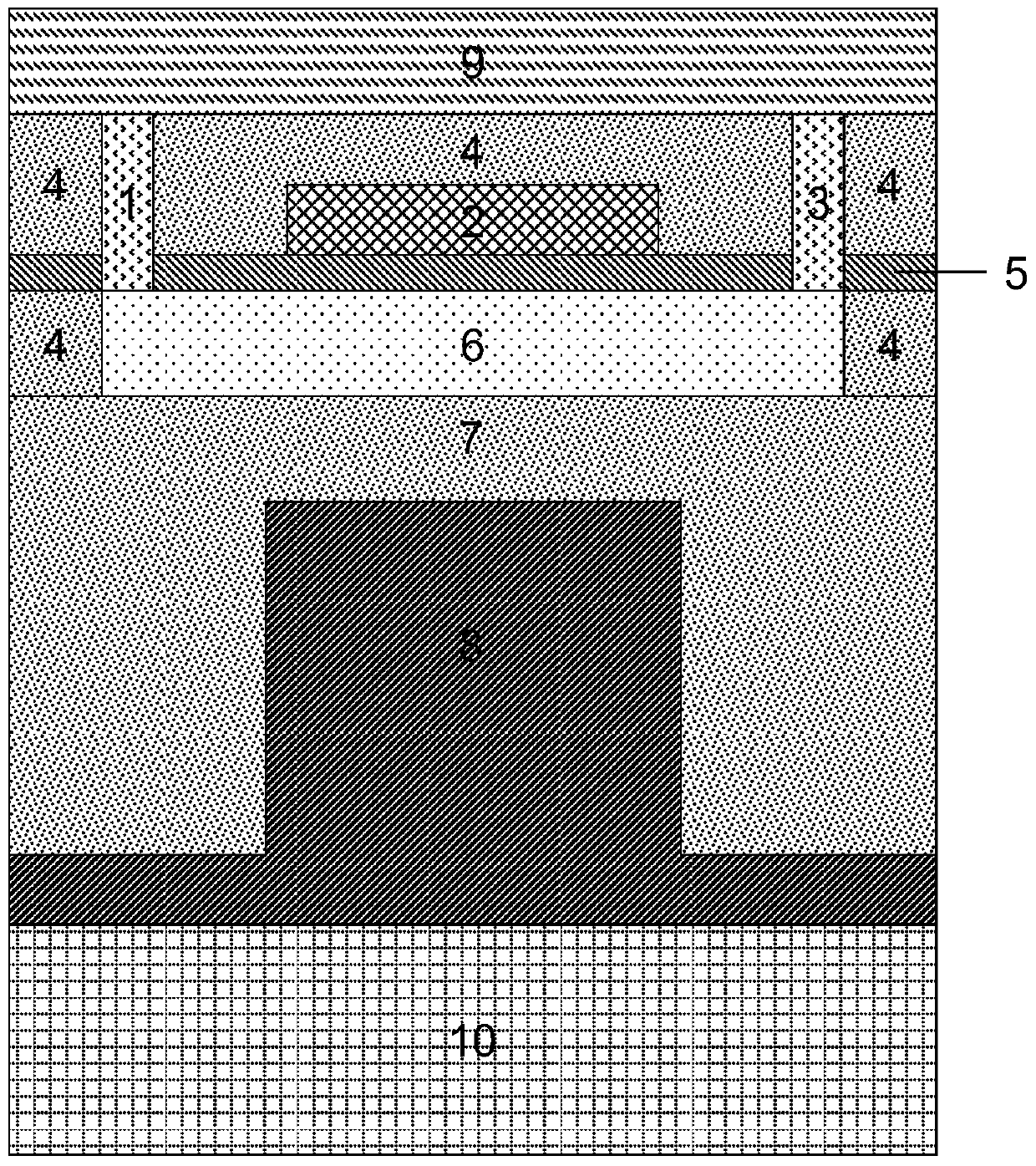
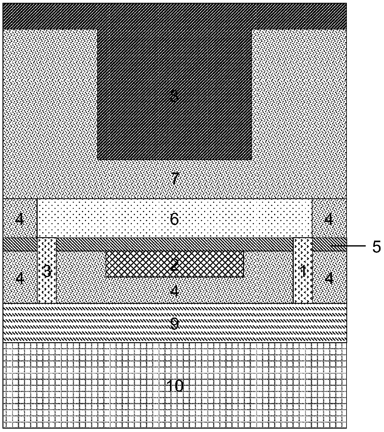
[0043] The present invention provides a high-performance SOI junction-free transistor with a non-single substrate insulating layer thickness. By applying an appropriate voltage bias to the voltage-adjustable substrate electrode 8, it can be equivalent to a double-gate or surrounding-gate structure, and the auxiliary gate electrode 2. Adjusting the distribution of carriers in the single crystal silicon thin film 6. Since the thickness of the insulating layer 7 of the SOI wafer is not a single value within a unit length of the device, the voltage bias on the voltage-adjustable substrate electrode 8 has different effects on the electric field distribution at different positions of the device, that is, in the SOI wafer The influence of the device part corresponding to the thinner part of the round insulating layer 7 is greater than the influence of the device part corresponding to the thicker part. When the device is turned off, the voltage bias on the voltage-adjustable substrate...


PUM


Abstract

The invention relates to a high-performance SOI junctionless transistor with a non-single substrate insulating layer thickness. The thickness of the SOI wafer insulating layer used is not a single value within the unit length of a transistor. The thickness of the insulating layer of the nearby SOI wafer significantly reduces the resistance of the source and drain regions, and significantly improves the forward conduction characteristics of the device. The present invention achieves local enhancement of the substrate voltage regulation effect by appropriately reducing the thickness of the insulating layer corresponding to the SOI wafer under the gate electrode, reduces the substrate voltage bias required for auxiliary gate control, and realizes low substrate voltage Voltage control. By optimizing the relative position and size of the thicker part and the thinner part of the insulating layer of the SOI wafer, the reverse direction caused by the inter-band tunneling near the junction between the device channel and the drain electrode when the gate electrode is reversed is effectively reduced. leakage current, so it is suitable for popularized applications.

Description

Technical field: [0001] The invention relates to the field of ultra-large-scale integrated circuit manufacturing, and relates to a specific structure, a structural unit and a manufacturing method of an array of high-performance SOI non-junction transistors with non-single substrate insulating layer thickness suitable for ultra-high-integration integrated circuit manufacturing. Background technique [0002] With the increasing integration of integrated circuits, the size of unit devices in the circuit continues to shrink. For the traditional integrated circuit unit, that is, the traditional metal oxide semiconductor field effect transistor (MOSFET), when the size reaches the nanometer level, on the one hand, the short channel effect has a significant impact on the device characteristics; on the other hand, in a few nanometers The manufacture of PN junctions under the scale has extremely high requirements for high technology. Compared with the traditional MOSFET, the multi-ga...

Claims


Application Information

Patent Timeline
Patent Type & Authority Patents(China)
IPC IPC(8): H01L29/78H01L29/06H01L29/423H01L21/28H01L21/336
CPCH01L21/28H01L29/0603H01L29/42368H01L29/78
Inventor 靳晓诗吴美乐刘溪揣荣岩
Owner SHENYANG POLYTECHNIC UNIV
Why Eureka
Try Eureka