Forming method of semiconductor structure

A semiconductor and graphic technology, applied in semiconductor devices, semiconductor/solid-state device manufacturing, transistors, etc., to improve performance and quality

Active Publication Date: 2015-03-18
SEMICONDUCTOR MANUFACTURING INTERNATIONAL (BEIJING) CORP +1
View PDF6 Cites 14 Cited by
  • Summary
  • Abstract
  • Description
  • Claims
  • Application Information

AI Technical Summary

Problems solved by technology

[0004] In the embedded flash memory device formed by the prior art, the performance of the storage unit in the storage area needs to be further improved

Method used


Image

  • Forming method of semiconductor structure
  • Forming method of semiconductor structure
  • Forming method of semiconductor structure

Examples


Embodiment Construction

[0027] As mentioned in the background art, the performance of the storage units in the storage area of ​​the embedded flash memory device still needs to be further improved.

[0028] Research has found that in the prior art, during the process of forming the storage unit of the embedded flash memory device, the top of the control gate of the storage unit is often damaged, resulting in the performance of the storage unit being affected.

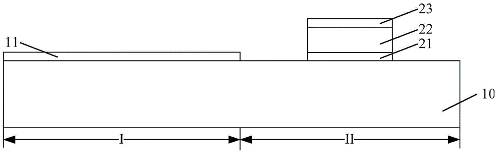
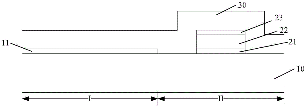
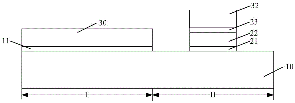
[0029] Please refer to Figure 1 to Figure 5 It is a structural schematic diagram of a method for forming an embedded flash memory device in the prior art.

[0030] Please refer to figure 1 , providing a semiconductor substrate 10, the semiconductor substrate has a first region I and a second region II, the first region I is a logic region, and the second region II is a storage region. There is an isolation structure (not shown in the figure) between the first region I and the second region II. A gate dielectric layer material layer 11 is f...


PUM


Abstract

Semiconductor devices and fabrication methods are provided. A semiconductor substrate includes a first region and a second region. A gate dielectric material layer is formed to cover the first region, and a control gate dielectric layer is formed over a surface portion of the second region. The control gate dielectric layer has a top surface higher than the gate dielectric layer. A gate material layer is conformally formed to cover an entire surface of the semiconductor substrate and has a top surface in the second region higher than a top surface in the first region. A first filling material layer is formed on the gate material layer. A first patterned mask layer is formed on the first filling material layer to form a gate on a gate dielectric layer in the first region. A control gate is formed on the control gate dielectric layer of the second region.

Description

technical field [0001] The invention relates to the technical field of semiconductors, in particular to a method for forming a semiconductor structure. Background technique [0002] In the current semiconductor industry, integrated circuit products can be mainly divided into three types: logic, memory and analog circuits, among which memory devices account for a considerable proportion of integrated circuit products. Among storage devices, the development of flash memory (flash memory, referred to as flash memory) is particularly rapid in recent years. Its main feature is that it can keep stored information for a long time without power on, and has many advantages such as high integration, fast access speed, easy erasure and rewriting, etc. The field has been widely used. [0003] With the development of semiconductor technology, storage devices are more widely used, and the storage device and other device regions need to be formed on a chip at the same time to form an emb...

Claims


Application Information

Patent Timeline
Patent Type & Authority Applications(China)
IPC IPC(8): H01L21/768H01L21/265
CPCH01L29/66825H01L29/788H01L21/28273H01L27/11531H10B41/48H01L29/40114H10B41/42
Inventor 王新鹏潘晶王琪宁先捷
Owner SEMICONDUCTOR MANUFACTURING INTERNATIONAL (BEIJING) CORP
Why Eureka
Try Eureka