Forming method of transistor

A technology of transistors and graphics, applied in the direction of semiconductor devices, semiconductor/solid-state device manufacturing, electrical components, etc., can solve the problems of high production cost and complicated production process, and achieve the effect of reducing production cost, simple forming process and high efficiency

Active Publication Date: 2015-03-18
SEMICON MFG INT (SHANGHAI) CORP
View PDF6 Cites 3 Cited by
  • Summary
  • Abstract
  • Description
  • Claims
  • Application Information

AI Technical Summary

Problems solved by technology

[0008] At present, there are mainly three kinds of mature SOI substrate formation processes, specifically SIMOX (Separation by Implanted Oxygen) process, silicon wafer bonding process, and Smart Cut (Smart Cut) process. The cost is relatively hi...

Method used


Image

  • Forming method of transistor
  • Forming method of transistor
  • Forming method of transistor

Examples


Embodiment Construction

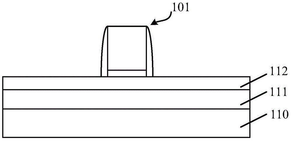
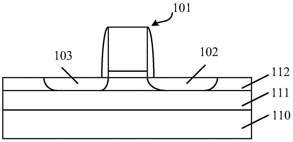
[0038] At present, SOI substrates are used as substrates in the production of fully depleted semiconductor-on-insulator transistors, and some fully depleted semiconductor-on-insulator transistors. The thickness uniformity is poor.

[0039]To this end, the present invention provides a method for forming a transistor, forming a first semiconductor layer and a second semiconductor layer on a substrate, etching the first semiconductor layer and the second semiconductor layer to form a semiconductor pattern, and removing the second semiconductor pattern The first semiconductor pattern at the bottom is formed into a cavity, and then an oxidation process is performed to form an oxide layer on the sidewall and bottom of the second semiconductor pattern and the surface of the substrate, and the oxide layer fills the cavity, and then the second A gate structure is formed on the surface of the two semiconductor patterns. The oxide layer is used as an insulating layer between the second ...


PUM

PropertyMeasurementUnit
Thicknessaaaaaaaaaa
Thicknessaaaaaaaaaa

Abstract

The invention provides a forming method of a transistor. The method comprises the following steps that a substrate is provided, and a first semiconductor layer is formed on the substrate; a second semiconductor layer is formed on the first semiconductor layer; the partial second semiconductor layer and the partial first semiconductor layer are etched, and a plurality of semiconductor patterns in parallel distribution in the first direction are formed; first semiconductor patterns formed at the bottom of the second semiconductor patterns are removed, and a cavity is formed; an oxidation process is carried out, oxidation layers are formed on the side wall and the bottom of second semiconductor patterns and the surface of the substrate, and the oxidation layers fully fill the cavity; the partial second semiconductor patterns are etched, the second semiconductor patterns are cut in the second direction, and a plurality of second grooves parallelly distributed in the second direction are formed in the second semiconductor patterns; first grooves and the second grooves are fully filled with insulation layers, and the surfaces of the insulation layer are aligned with the surfaces of the semiconductor patterns; grid electrode structures are formed on the surfaces of the broken semiconductor patterns. The forming method has the advantage that the manufacturing cost is reduced.

Description

technical field [0001] The invention relates to the field of semiconductor manufacturing, in particular to a method for forming a transistor. Background technique [0002] With the improvement of component density and integration of semiconductor devices, the gate size of transistors is getting smaller and smaller, and the smaller gate size of transistors will intensify the short channel effect, causing leakage current in transistors and affecting the electrical properties of semiconductor devices. performance. [0003] In order to overcome the short-channel effect of transistors and suppress leakage current, the prior art proposes a transistor device formed on an insulator, such as a fully-depleted semiconductor-on-insulator (FD-SOI, Fully-Depleted Semiconductor On Insulator) transistor, And Partly-Depleted Semiconductor On Insulator (PD-SOI, Partly-Depleted Semiconductor On Insulator) transistors. [0004] Figure 1 to Figure 2 It is a schematic cross-sectional structure...

Claims


Application Information

Patent Timeline
IPC IPC(8): H01L21/336H01L21/762
CPCH01L29/66553
Inventor 洪中山
Owner SEMICON MFG INT (SHANGHAI) CORP
Why Eureka
Try Eureka