Display base plate and preparation method thereof, and display device
A technology for display substrates and base substrates, which is applied in the direction of electrical components, electric solid devices, circuits, etc., can solve the problems of poor coverage characteristics, wrinkles, and fractures of the gate insulating layer, so as to reduce the deterioration of coverage characteristics and improve the open state. The effect of current
- Summary
- Abstract
- Description
- Claims
- Application Information
AI Technical Summary
Problems solved by technology
Method used
Image
Examples
Embodiment 1
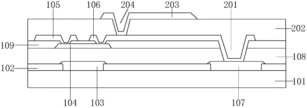
[0022] figure 1 It is a schematic structural diagram of a display substrate provided in Embodiment 1 of the present invention. Such as figure 1 As shown, the display substrate includes a base substrate 101 and gate lines and data lines located on the base substrate 101, the gate lines and the data lines define pixel units, and the pixel units include thin film transistors and pixel electrodes. The thin film transistor includes a gate, an active layer 104 , a source 105 and a drain 106 . An auxiliary layer 102 is further disposed on the base substrate 101, and a first groove is disposed on the auxiliary layer 102, and the gate and the gate line are located in the first groove. In this embodiment, the gate and the gate line are collectively referred to as a gate pattern 103, and the gate pattern 103 is located in the first groove, which can reduce the problem of the gate at the side wall due to the increase in the thickness of the gate layer. The covering properties of the i...
Embodiment 2
[0031] This embodiment provides a display device, including the display substrate provided in Embodiment 1. For details, please refer to the description in Embodiment 1 above, which will not be repeated here.
[0032] In the display device provided in this embodiment, the thin film transistor includes a gate, an active layer, and a source and drain, and an auxiliary layer is further arranged on the base substrate, and a first groove is arranged on the auxiliary layer, so that The gate and the gate line are located in the first groove, which can reduce the risk of poor coverage of the gate insulation layer at the sidewall or even wrinkles or fractures due to the increase in the thickness of the gate layer. In addition, due to the protection of the auxiliary layer, even if a thicker gate layer is used, a thinner gate insulating layer can be used, so that the on-state current of the thin film transistor can be increased.
Embodiment 3
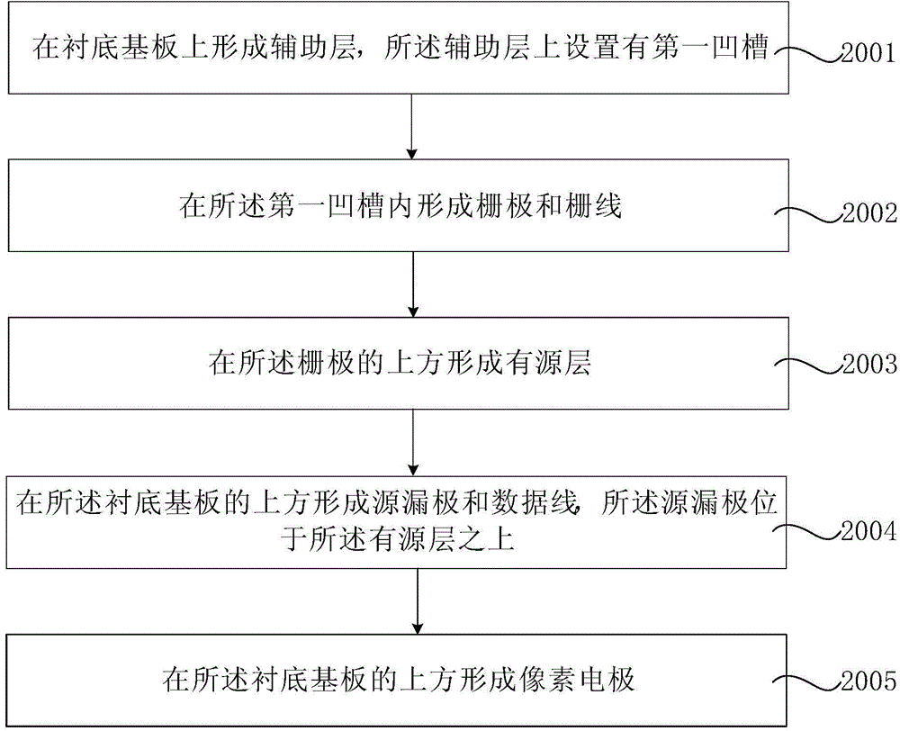
[0034] figure 2 It is a flow chart of a method for manufacturing a display substrate provided by Embodiment 3 of the present invention. Such as figure 2 As shown, the manufacturing method of the display substrate includes:
[0035] Step 2001, forming an auxiliary layer on the base substrate, the auxiliary layer is provided with a first groove.
[0036] image 3 It is a schematic diagram of forming the auxiliary layer in the third embodiment. Such as image 3 As shown, an auxiliary layer 102 is formed on a base substrate 101 , and a first groove 205 is disposed on the auxiliary layer 102 . Optionally, the auxiliary layer 102 is further provided with a second groove 206 .
[0037] Step 2002, forming gates and gate lines in the first groove.
[0038] Figure 4 It is a schematic diagram of forming gates and gate lines in Embodiment 3. Such as Figure 4As shown, gates and gate lines are formed in the first groove 205 . Optionally, a gate metal 107 is formed in the seco...
PUM
 Abstract
Description
Claims
Application Information
 - R&D
- Intellectual Property
- Life Sciences
- Materials
- Tech Scout
- Unparalleled Data Quality
- Higher Quality Content
- 60% Fewer Hallucinations
Browse by: Latest US Patents, China's latest patents, Technical Efficacy Thesaurus, Application Domain, Technology Topic, Popular Technical Reports.
© 2025 PatSnap. All rights reserved.Legal|Privacy policy|Modern Slavery Act Transparency Statement|Sitemap|About US| Contact US: help@patsnap.com


