
Method for manufacturing graphene gain coupling distributive feedback type silica based mixing laser

A distributed feedback and hybrid laser technology, which is applied to lasers, laser components, semiconductor lasers, etc., can solve problems such as material lattice mismatch, and achieve low scattering loss, simple process, and low cost.

Inactive Publication Date: 2015-01-28
INST OF SEMICONDUCTORS - CHINESE ACAD OF SCI
View PDF5 Cites 6 Cited by
  • Summary
  • Abstract
  • Description
  • Claims
  • Application Information

AI Technical Summary

Problems solved by technology

[0006] The object of the present invention is to provide a kind of manufacture method of graphene gain-coupling distributed feedback type silicon-based hybrid laser, III-V family material is a kind of good luminescent material, Si is a kind of good waveguide material, adopts bonding Combining them solves the material lattice mismatch problem introduced by direct epitaxy

Method used


Image

  • Method for manufacturing graphene gain coupling distributive feedback type silica based mixing laser
  • Method for manufacturing graphene gain coupling distributive feedback type silica based mixing laser
  • Method for manufacturing graphene gain coupling distributive feedback type silica based mixing laser

Examples


Embodiment Construction

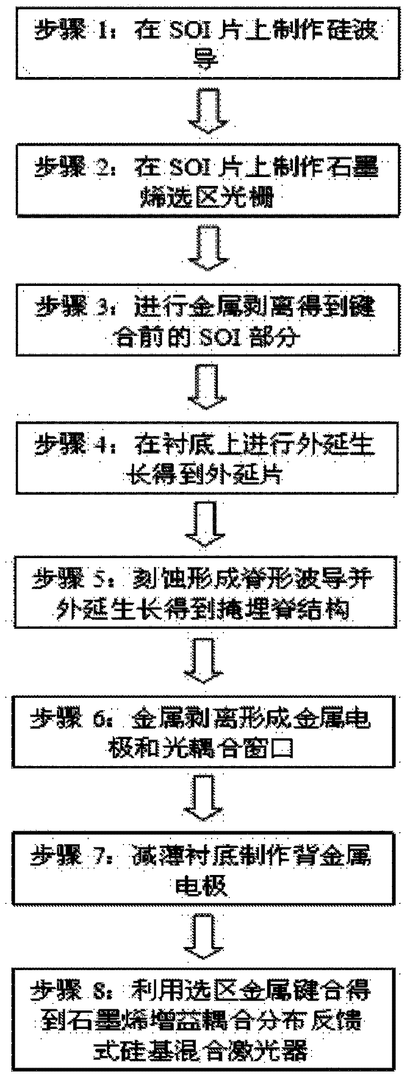
[0026] see figure 1 and refer to Figure 2-Figure 8 As shown, a method for manufacturing a graphene gain-coupled distributed feedback silicon-based hybrid laser of the present invention is described in detail. The specific implementation plan is introduced below:

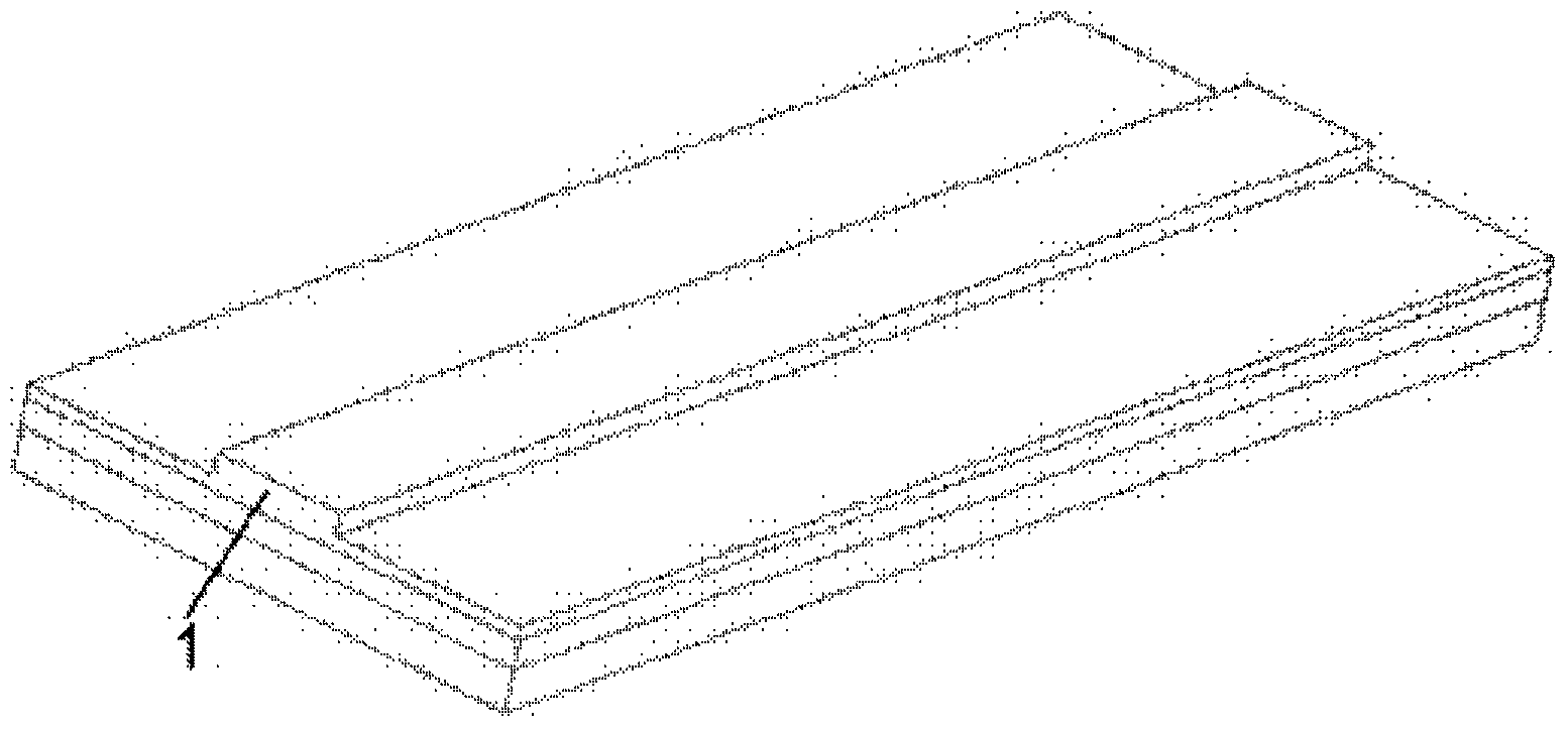
[0027] Step 1: Fabricate a silicon waveguide 1 on the top silicon layer of the SOI sheet by inductively coupled plasma etching (ICP), wherein the silicon waveguide has a width of 2 μm-5 μm and a height of 120nm-500nm, such as figure 2 shown;

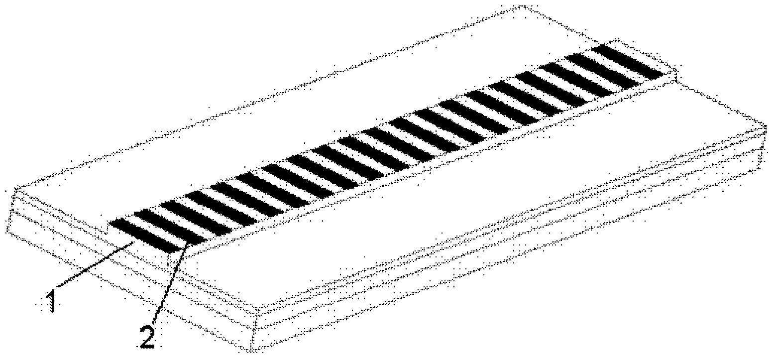
[0028] Step 2: Transfer large-area graphene to the SOI sheet after the silicon waveguide 1 is completed, and the number of transferred graphene layers is 1-5 layers. Calculation of the effective refractive index n of a graphene gain-coupled distributed feedback laser using finite-difference time-domain (FDTD) software eff , given the target wavelength λ, into the formula Λ = λ / 2n eff , to obtain the period Λ of the graphene grating. On the graphene-covered SOI sheet, a ...


PUM

PropertyMeasurementUnit
Widthaaaaaaaaaa

Abstract

A method for manufacturing a graphene gain coupling distributive feedback type silica based mixing laser. The method comprises the following steps of manufacturing silicon waveguides on top silicon of an SOI slice; manufacturing a graphene district grating on the SOI slice subjected to the manufacture of the silicon waveguides to form a chip; performing metal stripping to obtain the SOI part before bonding; sequentially growing a lower separation limit layer, an active area and an upper separation limit layer on a substrate in an epitaxial mode to form an epitaxial wafer; etching ridge waveguides; forming a layer of metal in an evaporation mode, and performing metal stripping to obtain an optical coupling window and a metal electrode; thinning the substrate and manufacturing a back metal electrode; performing metal bonding by means of selected districts to finishing manufacture. The method is simple in process, low in scattering loss and good in single-mode effect and has pure gains.

Description

technical field [0001] The invention belongs to the field of electronic devices, and in particular relates to a method for manufacturing a graphene gain coupling distributed feedback (DFB) silicon-based hybrid laser. The manufacturing process is simple, the cost is low, and the reliability is high. The coupled distributed feedback silicon-based hybrid laser is pure gain and reduces losses in single-mode lasers. Background technique [0002] In recent years, with the maturity of silicon photonics discrete devices, silicon-based optical interconnects have gradually become a research hotspot, but the lack of effective silicon-based light sources has become the biggest obstacle on the road to optoelectronic device integration. The reason is that the silicon material itself has an indirect band gap and low luminous efficiency, so a special structure must be sought or combined with other materials to realize a silicon-based light source. [0003] In a broad sense, silicon-based l...

Claims


Application Information

Patent Timeline
IPC IPC(8): H01S5/22H01S5/028
Inventor 任正良阚强袁丽君潘教青王圩
Owner INST OF SEMICONDUCTORS - CHINESE ACAD OF SCI
Learn More