
Method for manufacturing plated-through holes in HDI plate

A technology of metallized holes and manufacturing methods, which is applied to the formation of electrical connections of printed components, etc., can solve the problems of high production cost, long production process, and low efficiency, and achieve the effects of improving quality, increasing production efficiency, and simplifying the process flow

Inactive Publication Date: 2014-12-24
SHENZHEN SUNTAK MULTILAYER PCB
View PDF3 Cites 20 Cited by
  • Summary
  • Abstract
  • Description
  • Claims
  • Application Information

AI Technical Summary

Problems solved by technology

[0003] The present invention aims at the problems that when the aspect ratio of the holes in the existing HDI board is high, the metallization of the blind holes and the metallization of the through holes need to be carried out separately, resulting in too long production process, high production cost and low efficiency, and provides a Method that enables simultaneous metallization of blind vias and vias

Method used


Image

  • Method for manufacturing plated-through holes in HDI plate
  • Method for manufacturing plated-through holes in HDI plate
  • Method for manufacturing plated-through holes in HDI plate

Examples


Embodiment 1

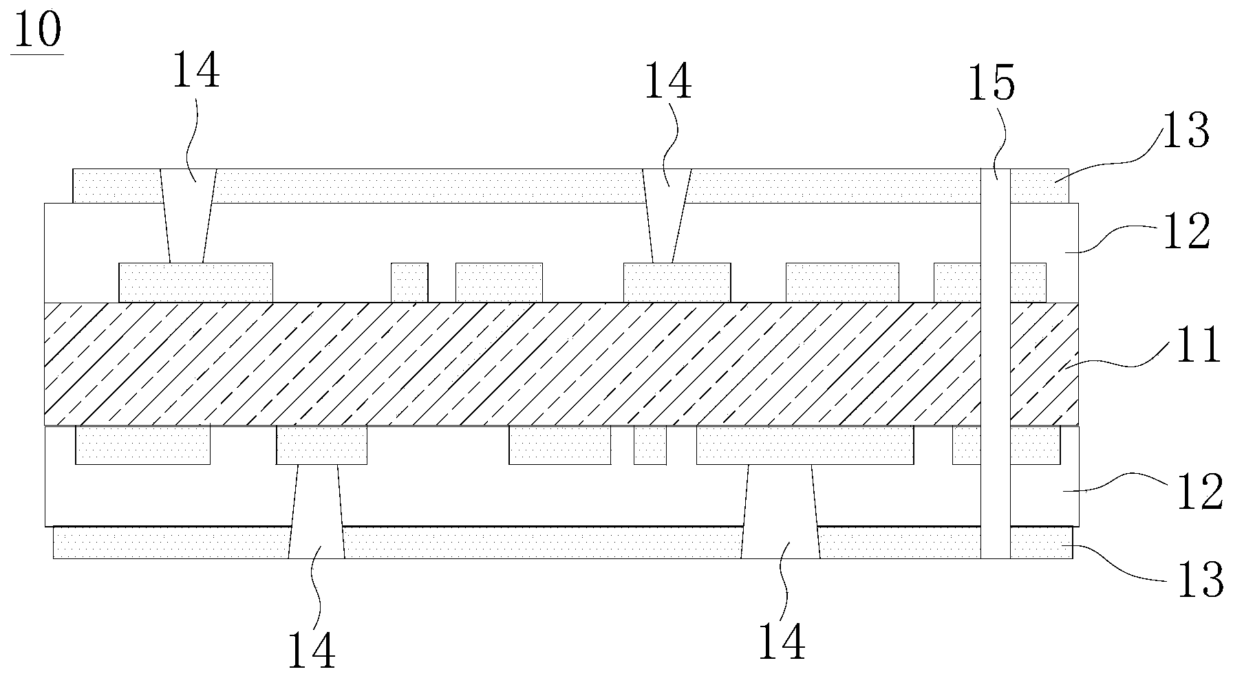
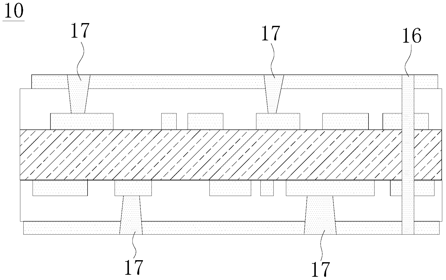
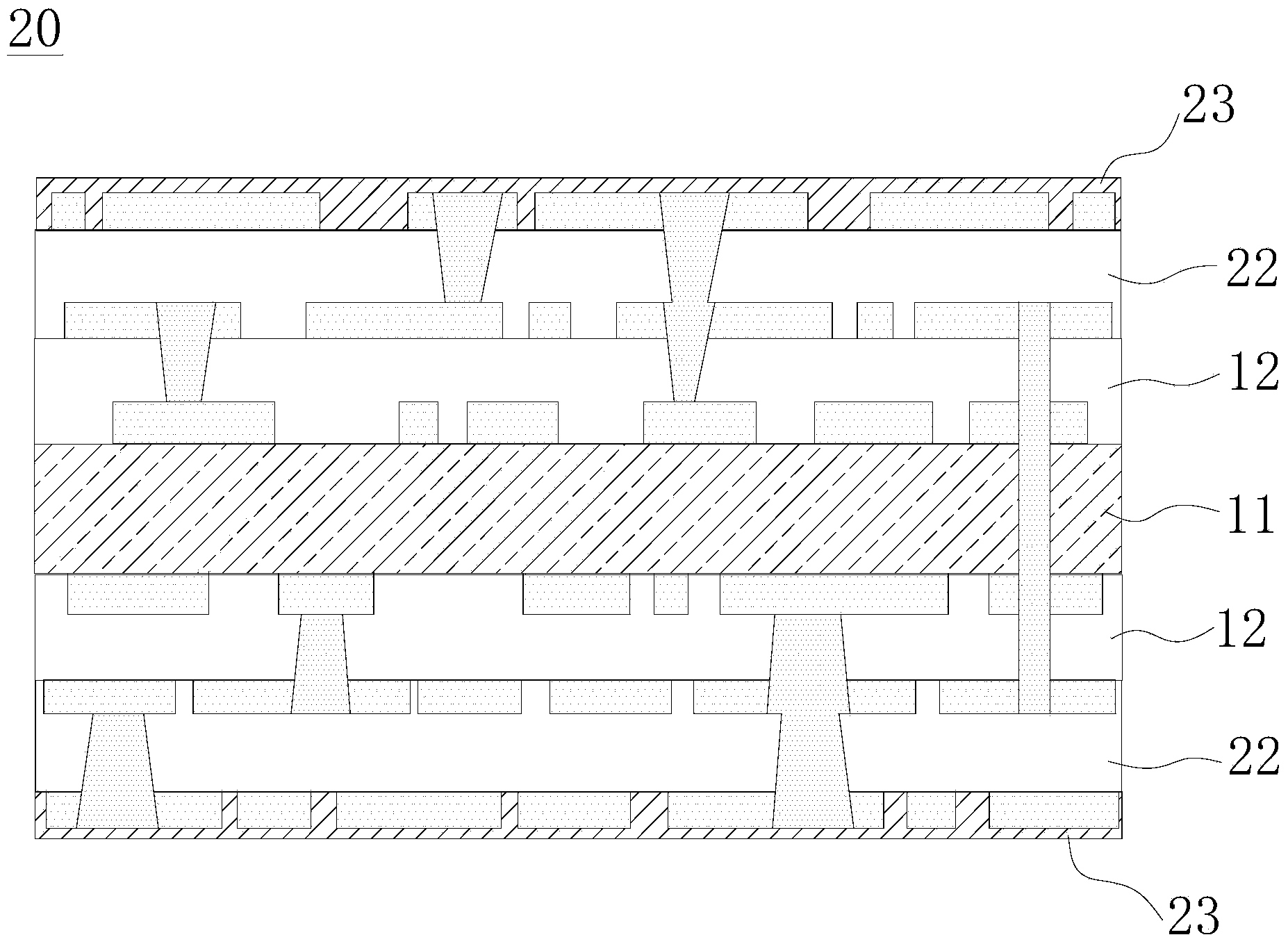
[0020] refer to Figure 1-3 , the preparation method of a kind of HDI plate 20 (six layers) that present embodiment provides, wherein included the method (the length and breadth of the metallized blind hole 17 of metallized blind hole 17) to make the method for metallized blind hole 17 and metallized through hole 16 simultaneously on HDI board 20 The ratio is 1.2:1, and the aspect ratio of the metallized via 16 is 10:1). The method specifically includes the following steps:

[0021] (1) According to the circuit board production process of the prior art, the circuit board raw material is cut to obtain the substrate, and then the inner layer pattern is transferred and etched on the substrate to form the inner layer circuit on the substrate to obtain the inner layer board 11 . After the inner layer board 11 is pre-pressed, the inner layer board 11 and the copper foil 13 are pressed together through the prepreg 12 to form the first multi-layer inner layer board 10 .

[0022] (2)...

Embodiment 2

[0039] This embodiment provides a method for preparing an HDI board (eight layers), which includes a method of simultaneously manufacturing metallized blind holes and metallized through holes on the HDI board. The method specifically includes the following steps:

[0040] Steps (1), (2) and (3) in this embodiment are the same as steps (1), (2) and (3) in Embodiment 1.

[0041] (4) After the first multi-layer inner layer board is pre-pressed, the first multi-layer inner layer board and the copper foil are pressed together through a prepreg to form a second multi-layer inner layer board. Then repeat the above step (2) to make metallized blind holes and metallized through holes on the second multilayer inner layer board. After making metallized blind vias and metallized through holes, slice analysis is done to inspect and evaluate the condition of metallized holes. Then repeat the operation of the above step (3) to make the inner layer circuit on the second multilayer inner lay...

Embodiment 3

[0046] This embodiment provides a method for manufacturing an HDI board (six layers), which includes a method of simultaneously manufacturing metallized blind holes and metallized through holes on the HDI board. The specific operation steps of this embodiment are basically the same as those of Embodiment 1, the difference being that in step (2), when using a vertical continuous electroplating line to perform electroplating for hole filling of the entire board, in the electroplating solution, Cu 2+ The concentration is 90g / L; H 2 SO 4 The concentration is 195g / L; Cl - The concentration of the lightening agent is 80ppm; the concentration of the leveling agent is 4mL / L, and the concentration of the brightening agent is 1.5mL / L.

[0047] According to the method of Example 3, 1000 HDI boards were produced, and the first multi-layer inner layer board after the whole board was filled and electroplated in the production process of each HDI board was sliced ​​and analyzed. The analy...


PUM

PropertyMeasurementUnit
thicknessaaaaaaaaaa
thicknessaaaaaaaaaa
thicknessaaaaaaaaaa

Abstract

The invention relates to the technical field of circuit board production, in particular to a method for manufacturing plated-through holes in an HDI plate. After blind holes and through holes are drilled in multiple inner-layer plates, inner-layer copper deposition and whole-plate hole filling electroplating are conducted so that the blind holes and the through holes can be metallized at the same time. A horizontal copper deposition electroplating wire is used during inner-layer copper deposition, a perpendicular continuous electroplating wire is used during whole-plate hole filling electroplating, the blind holes and the through holes can be metallized at the same time when the horizontal copper deposition electroplating wire and the perpendicular continuous electroplating wire are used in cooperation, and therefore the technological process can be simplified, production efficiency can be improved, and production cost can be reduced. Specific electroplate liquid is used during whole-plate hole filling electroplating, and therefore the quality of the metallized blind holes and the metallized through holes can be remarkably improved, and the metallized blind holes are prevented from cavities, fractures, poor hole filling and the like, the thickness of hole wall copper layers of the metallized through holes is 25 micrometers or higher, the thickness of electroplated copper on the surfaces of the inner-layer plates ranges from 35 micrometers to 45 micrometers, the requirements of a client are completely met, and manufacturing of circuits in the later procedure is completely achieved.

Description

technical field [0001] The invention relates to the technical field of circuit board production, in particular to a method for manufacturing metallized holes in an HDI board. Background technique [0002] HDI is the English abbreviation of High Density Interconnector. HDI boards are commonly referred to as high-density circuit boards. High-density interconnect (HDI) manufacturing is one of the fastest-growing fields in the printed circuit board industry. With the development needs of electronic products, the design and application of HDI boards are becoming more and more extensive. At present, for HDI boards with a blind hole aspect ratio below 1:1 and a through hole aspect ratio below 8:1, the holes can be metallized by simultaneously plating the entire board. However, for HDI boards with via holes with higher aspect ratios, if the holes are metallized by simultaneous electroplating of the entire board, it will be very easy to have voids and fractures in blind holes, and t...

Claims


Application Information

Patent Timeline
Patent Type & Authority Applications(China)
IPC IPC(8): H05K3/42C25D3/38
Inventor 韩启龙张军杰刘克敢
Owner SHENZHEN SUNTAK MULTILAYER PCB
Learn More