In2O3-WO3 oxide semiconductor acetone sensor, preparation method and application thereof
An oxide semiconductor, in2o3-wo3 technology, applied in textiles and papermaking, fiber processing, material resistance, etc., can solve the problems of high detection limit and low sensitivity of sensors, and achieve the effect of low detection limit, high sensitivity and favorable cost
- Summary
- Abstract
- Description
- Claims
- Application Information
AI Technical Summary
Problems solved by technology
Method used
Image
Examples
Embodiment 1
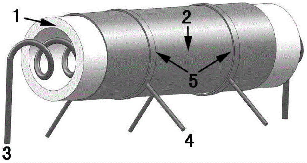
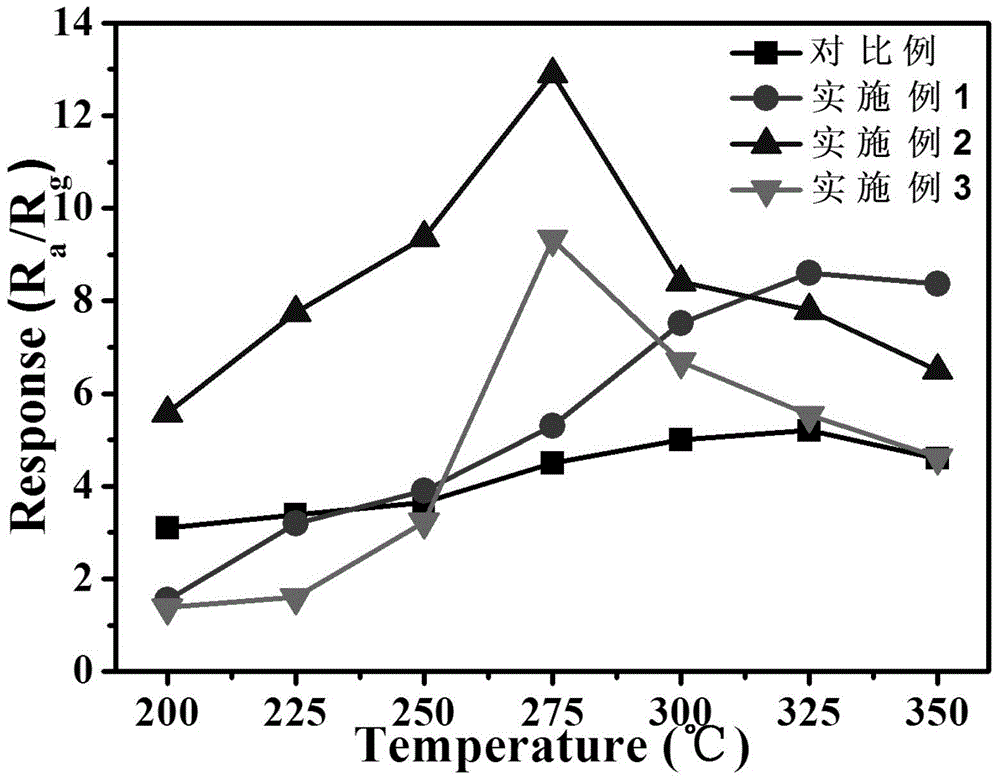
[0039] In with a molar ratio of 0.005:1 2 o 3 -WO 3 Oxide semiconductors are used as sensitive materials to make acetone sensors, and the manufacturing process is as follows
[0040] 1. First add 4mmol WCl 6 , 0.04mmol In(NO 3 ) 3 4.5H 2 0 and 1.25g polyvinylpyrrolidone were dissolved in the mixed solution of 9g dimethylformamide, 1g ethanol and 0.2g acetic acid, stirred for 4 hours to form a sol;
[0041] 2. Put the above solution into the electrospinning device, make the distance between the collecting plate and the spinneret 10cm, the applied voltage of the spinneret is +15kv, the collecting plate is grounded, and the material is collected after 3 hours of experiment;
[0042] 3. Put the collected materials into a high-temperature resistance furnace for calcination at 500°C for 120 minutes to obtain In 2 o 3 -WO 3 nanowire-sensitive materials. Take a small amount of sensitive material powder, drop it into deionized water at a mass ratio of 4:1, and grind it into a...
Embodiment 2
[0045] In with a molar ratio of 0.015:1 2 o 3 -WO 3 Oxide semiconductors are used as sensitive materials to make acetone sensors, and the manufacturing process is as follows
[0046] 1. First add 4mmol WCl 6 , 0.12mmol In(NO 3 ) 3 4.5H 2 0 and 1.25g polyvinylpyrrolidone were dissolved in the mixed solution of 9g dimethylformamide, 1g ethanol and 0.2g acetic acid, stirred for 4 hours to form a sol;
[0047] 2. Put the above solution into the electrospinning device, make the distance between the collecting plate and the spinneret 10cm, the applied voltage of the spinneret is +15kv, the collecting plate is grounded, and the material is collected after 3 hours of experiment;
[0048] 3. Put the collected materials into a high-temperature resistance furnace for calcination at 500°C for 120 minutes to obtain In 2 o 3 -WO 3 nanowire-sensitive materials. Take a small amount of sensitive material powder, drop it into deionized water at a mass ratio of 4:1, and grind it into a...
Embodiment 3
[0051] use In 2 o 3 with WO 3 In with a molar ratio of 0.03:1 2 o 3 -WO 3 Oxide semiconductors are used as sensitive materials to make acetone sensors, and the manufacturing process is as follows
[0052] 1. First add 4mmol WCl 6 , 0.24mmol In(NO 3 ) 3 4.5H 2 0 and 1.25g polyvinylpyrrolidone were dissolved in the mixed solution of 9g dimethylformamide, 1g ethanol and 0.2g acetic acid, stirred for 4 hours to form a sol;
[0053] 2. Put the above solution into the electrospinning device, make the distance between the collecting plate and the spinneret 10cm, the applied voltage of the spinneret is +15kv, the collecting plate is grounded, and the material is collected after 3 hours of experiment;
[0054] 3. Put the collected materials into a high-temperature resistance furnace for calcination at 500°C for 120 minutes to obtain In 2 o 3 -WO 3 nanowire-sensitive materials. Take a small amount of sensitive material powder, drop it into deionized water at a mass ratio of...
PUM
 Abstract
Description
Claims
Application Information
 - Generate Ideas
- Intellectual Property
- Life Sciences
- Materials
- Tech Scout
- Unparalleled Data Quality
- Higher Quality Content
- 60% Fewer Hallucinations
Browse by: Latest US Patents, China's latest patents, Technical Efficacy Thesaurus, Application Domain, Technology Topic, Popular Technical Reports.
© 2025 PatSnap. All rights reserved.Legal|Privacy policy|Modern Slavery Act Transparency Statement|Sitemap|About US| Contact US: help@patsnap.com


