
A kind of preparation method of millimeter wave rf MEMS switch

A millimeter wave and switching technology, which is applied in the field of MEMS device manufacturing, can solve the problems of low switch yield, difficulty in achieving low insertion loss and high isolation, and short service life, and achieves the effect of a simple method.

Active Publication Date: 2016-09-21
NO 54 INST OF CHINA ELECTRONICS SCI & TECH GRP
View PDF5 Cites 0 Cited by
  • Summary
  • Abstract
  • Description
  • Claims
  • Application Information

AI Technical Summary

Problems solved by technology

[0004] The existing millimeter-wave RF MEMS switch preparation method has low yield and short service life of the switch; and in the millimeter-wave frequency band, it is difficult to achieve low insertion loss and high isolation at the same time
Reducing the insertion loss of RF MEMS switches while improving isolation, yield and lifetime is a big challenge for MEMS manufacturing

Method used


Image

  • A kind of preparation method of millimeter wave rf MEMS switch

Examples


Embodiment Construction

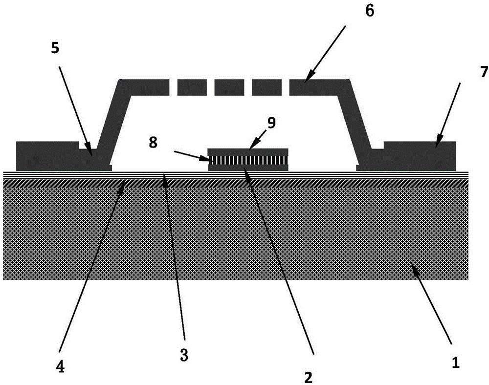
[0037] Below, combine figure 1 The present invention is further described.

[0038] A preparation method of a millimeter-wave RF MEMS switch, the millimeter-wave RF MEMS switch includes a switch substrate, a CPW pattern on the switch substrate and a thin film microbridge 6, the CPW pattern includes an RF transmission line 2 and is located on both sides of the RF transmission line The ground wire 7 specifically includes the following steps:

[0039] (1) On the surface of the high-resistance silicon wafer 1, a layer of polysilicon 4 is grown by PECVD process, and then a layer of silicon dioxide 3 is grown on the polysilicon to obtain a switch substrate;

[0040] (2) cleaning and drying the silicon wafer after step (1);

[0041] (3) Send the silicon chip after step (2) into the magnetron sputtering station, and sputter the titanium-tungsten-gold film layer;

[0042] (4) take out the silicon chip after step (3) processing, cover the position other than the line pattern that nee...


PUM

PropertyMeasurementUnit
isolationaaaaaaaaaa

Abstract

The invention relates to the field of MEMS device manufacturing, in particular to a method for preparing a millimeter-wave RF MEMS switch, which mainly includes the growth of polysilicon and silicon dioxide on the surface of a high-resistance silicon wafer, silicon wafer cleaning, CPW pattern production, and silicon nitride on the RF transmission line. Fabrication of the insulating layer, fabrication of the conductor layer on the silicon nitride insulating layer of the RF transmission line, fabrication of the sacrificial layer, fabrication of the thin film micro-bridge, release of the sacrificial layer, annealing, and performance testing steps. The millimeter-wave RF MEMS switch prepared by adopting the technical solution of the present invention has a relatively high yield rate, a relatively long switch life, low insertion loss and high isolation in the millimeter-wave frequency band, and a simple sacrificial layer planarization method during processing .

Description

technical field [0001] The invention relates to the field of MEMS device manufacture, in particular to a preparation method of a millimeter-wave RF MEMS switch. Background technique [0002] Electronic equipment is gradually developing in terms of functional diversification, miniaturization, light weight, and high frequency. Due to the advantages of miniaturization, intelligence, multi-function and high integration, RF MEMS devices have been more and more widely used. [0003] RF MEMS switch is one of the most basic components in MEMS radio frequency devices, and it is also the core device of radio frequency circuits. It can be used alone or combined with other microwave circuits or devices to form other composite devices, such as phase shifters, Reconfigurable antennas, filters, etc. RF MEMS switches have excellent performance in terms of insertion loss, isolation, frequency, and linearity, so they are widely used in systems such as satellite communications, navigation, a...

Claims


Application Information

Patent Timeline
Patent Type & Authority Patents(China)
IPC IPC(8): B81C1/00
Inventor 党元兰赵飞梁广华刘晓兰徐亚新董自强唐小平朱二涛杨宗亮严英占王康
Owner NO 54 INST OF CHINA ELECTRONICS SCI & TECH GRP
Learn More