
Asymmetric Schottky source drain transistor and preparing method thereof

An asymmetric, Schottky potential technology, applied in transistors, semiconductor/solid-state device manufacturing, semiconductor devices, etc., can solve problems such as the complexity of GAA source-drain design, solve thermal stability problems, suppress short-channel effects, and improve integration degree of effect

Active Publication Date: 2014-11-05
PEKING UNIV
View PDF2 Cites 7 Cited by
  • Summary
  • Abstract
  • Description
  • Claims
  • Application Information

AI Technical Summary

Problems solved by technology

In addition, the introduction of nanowires makes the source and drain design of GAA more complex than planar devices and multi-gate devices

Method used


Image

  • Asymmetric Schottky source drain transistor and preparing method thereof
  • Asymmetric Schottky source drain transistor and preparing method thereof
  • Asymmetric Schottky source drain transistor and preparing method thereof

Examples


Embodiment Construction

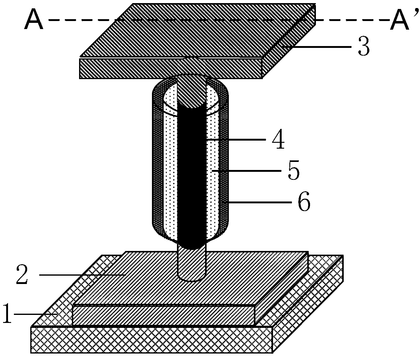
[0041] The present invention provides a MOS transistor with a novel structure, specifically a gate-around MOS transistor combined with a vertical channel and an asymmetric Schottky barrier source / drain structure (such as figure 1shown), including a ring-shaped semiconductor channel 4 in a vertical direction, a ring-shaped gate electrode 6, a ring-shaped gate dielectric layer 5, a source region 2, a drain region 3, and a semiconductor substrate 1; wherein, the source The region 2 is located at the bottom of the vertical channel 4 and is in contact with the substrate 1. The drain region 3 is located at the top of the vertical channel 4. The gate dielectric layer 5 and the gate electrode 6 surround the vertical channel 4 in a ring shape; the source region 2 and the The drain region 3 forms Schottky contacts with different barrier heights with the channel 4 respectively.

[0042] The source region and the drain region can be any metal with good conductivity or a compound formed of...


PUM


Abstract

The invention discloses a ring gate MOS transistor combining a vertical channel and an asymmetric Schottky barrier source / drain structure. The ring gate MOS transistor comprises the ring semiconductor channel (4) in the vertical direction, a ring gate electrode (6), a ring gate dielectric layer (5), a source region (2), a drain region (3) and a semiconductor substrate (1), wherein the source region is located at the bottom of the vertical channel (4) and connected with a substrate, the drain region is located on the top of the vertical channel, the gate dielectric layer and the gate electrode annularly surround the vertical channel, Schottky contacts with different barrier heights can be formed by the source region and the channel and the drain region and the channel respectively, and the source region and the drain region are made of different metal materials. The ring gate MOS transistor is compatible with an existing CMOS technology, various advantages of the traditional GAA are reserved, the leakage current is reduced through the asymmetric Schottky barrier source / drain structure, the technology requirement is lowered, the limitation of processing photoetching extremity is broken through via the vertical channel and the ring gate structure, and the integrity is improved.

Description

technical field [0001] The invention belongs to the field of field-effect transistor logic devices and circuits in CMOS ultra-large integrated circuits (ULSI), in particular to a gate-around MOS transistor combined with a vertical channel and an asymmetric Schottky barrier source / drain structure and a preparation method thereof . Background technique [0002] Driven by Moore's Law, the feature size of traditional MOSFETs has been shrinking, and now it has entered the nanometer scale. As a result, the negative effects of short-channel effects on devices have become more serious. The effects of leakage-induced barrier reduction and band-band tunneling increase the off-state leakage current of the device. In the research on new device structures, the source-drain doped Gate All Around transistor (GAA) structure is currently the most concerned one. GAA devices have better gate control characteristics, which can meet the sharpest characteristic requirements, so as to meet the n...

Claims


Application Information

Patent Timeline
Patent Type & Authority Applications(China)
IPC IPC(8): H01L29/78H01L29/786H01L29/47H01L21/336
CPCH01L29/1079H01L29/42356H01L29/47H01L29/66477H01L29/66969H01L29/7828H01L29/7839
Inventor 孙雷徐浩张一博韩静文王漪张盛东
Owner PEKING UNIV
Learn More