POP packaging structure

A technology of packaging structure and packaging body, which is applied in the direction of electrical components, electrical solid devices, circuits, etc., to achieve the effect of reducing warpage

Inactive Publication Date: 2014-10-01
NANTONG FUJITSU MICROELECTRONICS
View PDF10 Cites 0 Cited by
  • Summary
  • Abstract
  • Description
  • Claims
  • Application Information

AI Technical Summary

Problems solved by technology

Package warpage is one of the problems that has to be considered and solved. At present, proper material selection and design of the upper and lower molding compound layers is one of the main methods to solve this problem, but the electrical connection of the upper and lower molding compound layers is a thorny issue.

Method used


Image

  • POP packaging structure
  • POP packaging structure
  • POP packaging structure

Examples


Embodiment 1

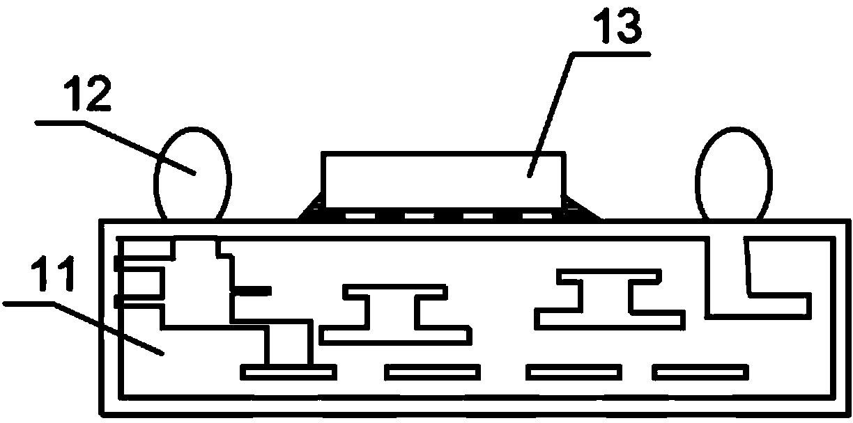
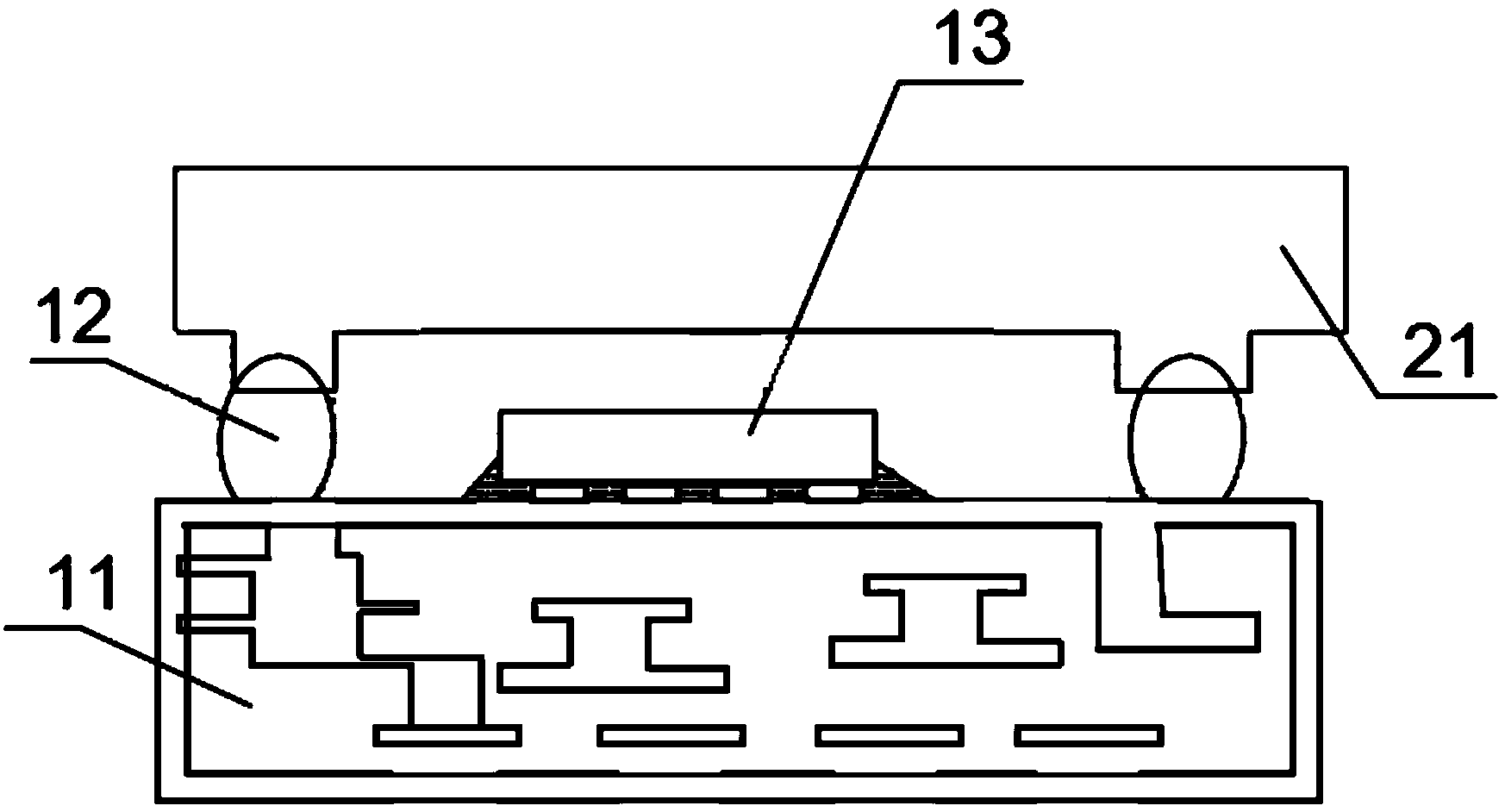
[0036] Such as figure 1 As shown, first, a substrate 11 is provided, a chip 13 is placed on the upper surface of the substrate 11, and the chip 13 is soldered on the substrate by a reflow soldering technique, and the chip 13 and the substrate 11 pass through the bottom Filling technology is used for reinforcement, and the underfilling can use molded underfilling technology or capillary underfilling technology.

[0037] Optionally, before the next step, a first solder ball 12 is formed on the upper surface of the substrate 11 or provided with a first solder ball on the surface of the substrate; the first solder ball on the upper surface of the substrate is used for contact with the upper package body Connect to realize the electrical interconnection between the upper package and the lower package. The first solder ball 12 on the upper surface of the substrate can be soldered on the upper surface of the substrate after the chip is packaged, or directly on the surface of the substrat...

Embodiment 2

[0046] Such as figure 1 As shown, first, a substrate 11 is provided, a chip 13 is placed on the upper surface of the substrate 11, and the chip 13 is soldered on the substrate by reflow soldering technology, and the chip 13 and the substrate 11 pass through the bottom Filling technology for reinforcement, where the underfilling can be molded underfilling technology or capillary underfilling technology; the first solder ball on the upper surface of the substrate can be set when the substrate is provided, or after the chip is soldered The upper surface of the substrate is provided with first solder balls.

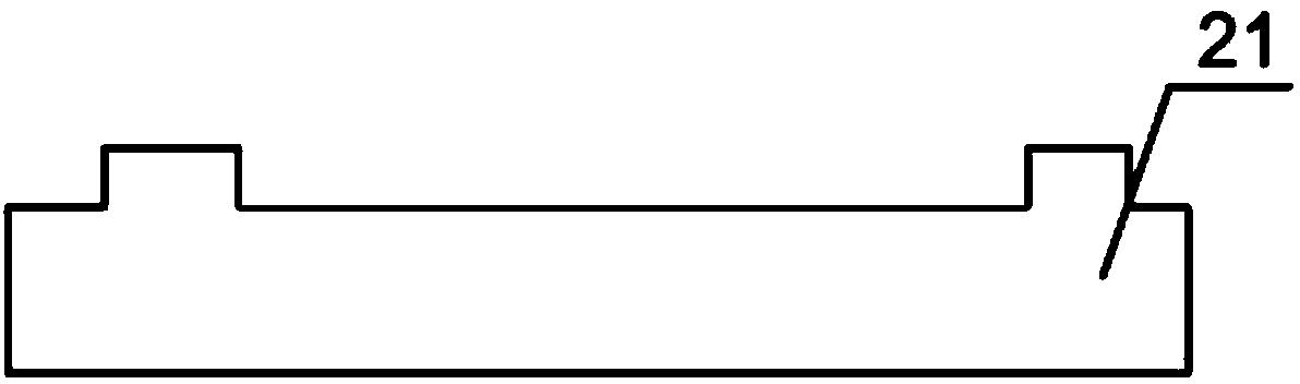
[0047] Subsequently, a metal strip 31 is provided, and the metal strip is subjected to photolithography and / or etching to form Figure 7 In the shape shown, metal bumps are formed on one side of the metal strip, and windings are also formed on the side where the metal bumps are formed.

[0048] The side of the metal strip with bumps and windings is facing down to the substrate, an...


PUM


Abstract

The invention provides a POP packaging structure. The POP packaging structure at least comprises an upper packaging body and a lower packaging body, wherein the upper packaging body and the lower packaging body are in butt joint. The lower packaging body comprises a substrate, metal salient points, a plastic packaging material layer, a chip, first welded balls and second welded balls. The first welded balls are arranged on the upper surface of the substrate. The metal salient points are directly connected to the top portions of the first welded balls. The chip is arranged on the upper surface of the substrate in an inversion mode through reflow soldering. The plastic packaging material layer is located on the upper surface of the substrate and covers the chip, the first welded balls and the metal salient points, and the top faces of the metal salient points are exposed out of the plastic packaging material layer. The second welded balls are arranged on the lower surface of the substrate. According to the POP packaging structure, electric connection is achieved without mechanical methods of drilling, plastic packaging material grinding and the like, the metal salient points are formed by metal strips with low cost through corrosion, grinding and other processes, electric connection serving as a connecting link is achieved, warping of the plastic packaging material layer is reduced, efficiency of electric connection is improved, and cost is reduced.

Description

Technical field [0001] The invention relates to a semiconductor packaging structure, in particular to a POP packaging structure. Background technique [0002] As the main method of packaging high-density integration, PoP (package on package, stacked packaging) has received more and more attention. In the POP structure, the memory chip is usually connected to the substrate by bonding, and the application processor chip is connected to the substrate by flip-chip. The memory chip package is directly stacked on the application processor package, and they are often soldered with solder balls. connection. In this way, the upper and lower structure reduces the interconnection distance of the two chips to save space and obtain better signal integrity. As the connection between the memory chip and the logic chip tends to be higher density and the overall thickness is getting thinner and thinner, the POP structure of the traditional package has been very limited. The warpage of the pack...

Claims


Application Information

Patent Timeline
Patent Type & Authority Applications(China)
IPC IPC(8): H01L23/31
CPCH01L2224/16227H01L2224/32225H01L2224/48227H01L2224/73204H01L2225/1023H01L2225/1041H01L2225/1058H01L2924/15311H01L2924/15321H01L2924/15331H01L2924/1815H01L2924/3511H01L2224/16225H01L2924/00
Inventor 张卫红张童龙
Owner NANTONG FUJITSU MICROELECTRONICS
Why Eureka
Try Eureka