Package substrate and manufacturing method thereof, and substrate assembly

A technology for encapsulating substrates and manufacturing methods, which is applied in the direction of printed circuits, electrical components, and circuit devices connected to non-printed electrical components, to achieve the effects of reliable structure, low manufacturing cost, and reduced failure risk

Inactive Publication Date: 2014-09-24
SHENNAN CIRCUITS
View PDF6 Cites 5 Cited by
  • Summary
  • Abstract
  • Description
  • Claims
  • Application Information

AI Technical Summary

Problems solved by technology

[0003] Embodiments of the present invention provide a packaging substrate and its manufacturing method and substrate assembly, so as to solve the defects caused by the electromagnetic shielding of the circuit board by the shielding cover in the prior art

Method used


Image

  • Package substrate and manufacturing method thereof, and substrate assembly
  • Package substrate and manufacturing method thereof, and substrate assembly
  • Package substrate and manufacturing method thereof, and substrate assembly

Examples


Embodiment 1

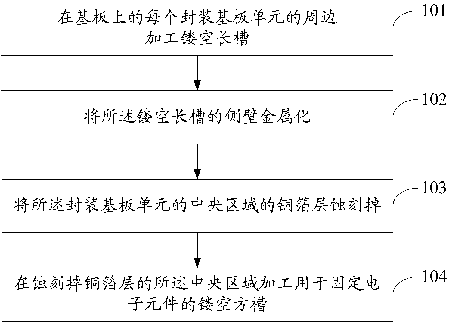
[0021] Please refer to figure 1 , an embodiment of the present invention provides a method for manufacturing a packaging substrate, including:

[0022] 101. Process hollow long grooves on the periphery of each packaging substrate unit on the substrate.

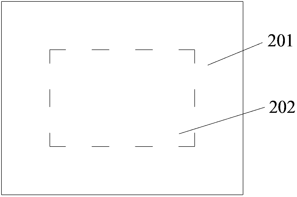
[0023] In this embodiment, the processing of the packaging substrate unit starts from a larger substrate, such as a double-sided copper-clad laminate. Several regularly arranged packaging substrate units are planned on the larger substrate. The plurality of packaging substrate units are arranged in an array, horizontally in rows and vertically in columns.

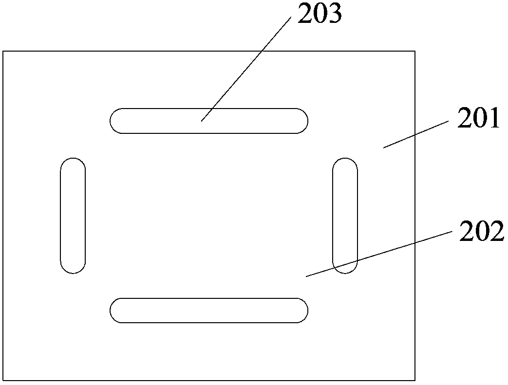
[0024] figure 2 A package substrate unit 202 on the substrate 201 is shown, and the dotted line box in the figure is the boundary of the package substrate unit 202 . In this step, if image 3 As shown, the hollow long grooves 203 can be processed along the dotted square frame on the periphery of the package substrate unit 202 , specifically, four hollow long grooves 2...

Embodiment 2

[0039] Please refer to Figure 10 The embodiment of the present invention provides a packaging substrate unit 202, the central area of ​​the packaging substrate unit 202 is provided with a hollowed out square groove 209 for fixing electronic components, and the surrounding side walls of the packaging substrate unit 202 are processed for The metallization layer 205 for electromagnetic shielding of the electronic components.

other Embodiment approach

[0040]In other implementation manners, the four corner portions of the packaging substrate unit 202 may be respectively processed with metallized through holes 204 . A layer of nickel-gold or nickel-palladium-gold may be plated on the copper foil layer on the sealing-rotation substrate unit 202 and the surrounding sidewalls.

[0041] Please refer to Figure 11 , the embodiment of the present invention also provides a substrate assembly, including: the packaging substrate unit 202 as described above, the electronic components 301 embedded in the hollow square grooves opened by the packaging substrate unit 202, and respectively press-fitted on the packaging substrate unit 202. The upper and lower substrates 302 on both sides of the packaging substrate unit 202 are packaged, and the electronic components 301 are electrically connected to the circuit patterns on the upper substrate or the lower substrate.

[0042] As above, the embodiment of the present invention provides a packa...


PUM


Abstract

A manufacturing method of a package substrate comprises: fabricating a hollowed-out elongated slot on the periphery of each package substrate unit on a substrate; metallizing the sidewalls of the hollowed-out elongated slot; etching off a copper foil layer at the central area of each package substrate unit; and fabricating, at the central area where the copper foil layer is etched off, a hollowed-out square groove for securing an electronic element. Further provided are a corresponding package substrate unit and a substrate assembly. In the technical solution of the present invention, sidewalls on the periphery of the package substrate unit are metallized to form a metal shielding layer, which easily and reliably implements electromagnetic shielding on the electronic element without the need of adding a shielding hood; in this way, the thickness of the package substrate is not increased, the universality of the product is not reduced, and the structure is reliable, thereby reducing the ineffectiveness risk; moreover, the cost is low.

Description

technical field [0001] The invention relates to the technical field of circuit board processing, in particular to a packaging substrate, a manufacturing method thereof, and a substrate assembly. Background technique [0002] Existing embedded circuit boards are usually manufactured by making slots on the circuit board, inserting electronic components such as chips into the slots and fixing them. The electronic components embedded in this kind of circuit board will be subject to external electromagnetic interference and cannot work in an optimal state. In the prior art, a method of adding a shielding cover to the circuit board is generally adopted to avoid electromagnetic interference. However, the shielding cover will increase the thickness of the circuit board, reduce the versatility of the product, and is not conducive to the development of miniaturization, and the shielding cover is not reliable enough, and there is a risk of failure such as displacement or falling off. ...

Claims


Application Information

Patent Timeline
Patent Type & Authority Applications(China)
IPC IPC(8): H05K3/00H05K3/30H05K1/02H05K1/18
CPCH05K3/30H05K1/02H05K1/185H05K1/0218H05K3/0047H05K2201/09981
Inventor 徐艺林高成志郑仰存谷新黄良松
Owner SHENNAN CIRCUITS
Why Eureka
Try Eureka