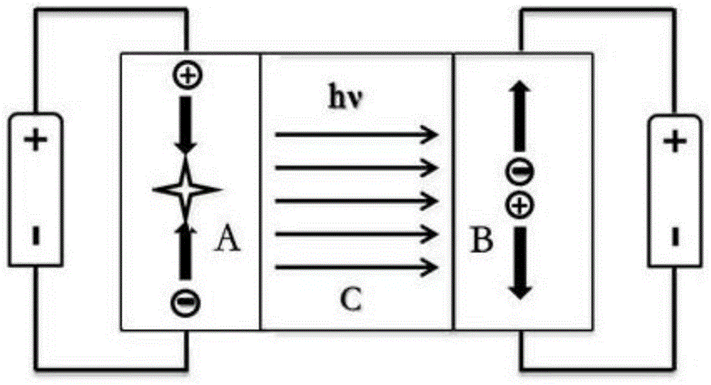
Optical coupler and preparation method for same
An optocoupler device and photosensitive technology, applied in the field of optoelectronics, can solve the problems of photosensitive effect change, influence signal conduction, small current transmission, etc., and achieve the effect of enhancing luminous intensity, expanding the range of color coordinates, and weakening the requirements of the light source.
- Summary
- Abstract
- Description
- Claims
- Application Information
AI Technical Summary
Problems solved by technology
Method used
Image
Examples
Embodiment 1
[0056] This embodiment provides an optocoupler device, such as the attached figure 2 As shown, it includes a luminescent film group A, a transparent electrical insulating isolation layer C, and a photosensitive thin film group B sequentially stacked on the substrate 1, and the electrode close to the electrical insulating isolation layer C in the luminescent film group A and photosensitive film group B is The same or different transparent electrodes.
[0057] The substrate 1 may be a glass substrate or a polymer substrate, and a flexible polyimide substrate is preferred in this embodiment.
[0058] The light-emitting film group A is preferably an organic light-emitting diode, which can be an organic small molecule light-emitting device or a polymer light-emitting device, including a first electrode 41 of the light-emitting film group, a light-emitting functional layer 42, and a second electrode 43 of the light-emitting film group. Such as Figure 4 As shown, the light-emitti...
Embodiment 2
[0090] This embodiment provides an optocoupler device, such as the attached image 3 As shown, the photosensitive thin film group B, the electrical insulation isolation layer C and the light emitting thin film group A are sequentially prepared on the substrate 1 from bottom to top. The specific preparation method is:
[0091] S1. The second electrode of the photosensitive thin film group, the first electrode pin of the photosensitive thin film group, the first electrode pin of the light emitting thin film group, and the pin of the light emitting thin film group are directly formed on the substrate 1 by using a magnetron sputtering process and a mask. the second electrode pin;
[0092] The substrate is preferably a flexible polyimide substrate, and the second electrode of the photosensitive film group is preferably an aluminum electrode with a thickness of 100 nm.
[0093] S2. Form a photosensitive functional layer and a first electrode of the photosensitive thin film group o...
Embodiment 3
[0108] This embodiment provides an optocoupler device. The specific structure and preparation method are the same as those in Embodiment 2. The only difference is that in this embodiment, the photosensitive functional layer further includes a second p-type semiconductor disposed on both sides of the photosensitive layer. layer and a second n-type semiconductor layer, and the second p-type semiconductor layer is arranged close to the light emitting thin film group.
[0109] The second n-type semiconductor layer is an n-type semiconductor material layer selected from but not limited to TiO 2 , ZnO and other inorganic semiconductor materials with large electron mobility, TiO is preferred in this embodiment 2 layer with a thickness of 150 nm.
[0110] The second p-type semiconductor layer is a p-type semiconductor material layer, selected from but not limited to organic semiconductor materials polytriarylamine (PTAA), 2,2',7,7'-tetrabromo-9,9'-spiro 2. Tris(4-iodophenyl)amine (S...
PUM
 Abstract
Description
Claims
Application Information
 - R&D
- Intellectual Property
- Life Sciences
- Materials
- Tech Scout
- Unparalleled Data Quality
- Higher Quality Content
- 60% Fewer Hallucinations
Browse by: Latest US Patents, China's latest patents, Technical Efficacy Thesaurus, Application Domain, Technology Topic, Popular Technical Reports.
© 2025 PatSnap. All rights reserved.Legal|Privacy policy|Modern Slavery Act Transparency Statement|Sitemap|About US| Contact US: help@patsnap.com


