
Touch substrate, manufacturing method thereof, and touch screen using the touch substrate

A substrate and touch technology, applied in the input/output process of data processing, instruments, electrical digital data processing, etc., can solve the problem of reduced conductivity of the grid-shaped conductive layer, achieve low resistivity, simplify the process, and improve The effect of conductivity

Active Publication Date: 2017-11-21
ANHUI JINGZHUO OPTICAL DISPLAY TECH CO LTD
View PDF5 Cites 1 Cited by
  • Summary
  • Abstract
  • Description
  • Claims
  • Application Information

AI Technical Summary

Problems solved by technology

The oxidation of the conductive material will lead to a decrease in the conductivity of the grid-shaped conductive layer.

Method used


Image

  • Touch substrate, manufacturing method thereof, and touch screen using the touch substrate
  • Touch substrate, manufacturing method thereof, and touch screen using the touch substrate
  • Touch substrate, manufacturing method thereof, and touch screen using the touch substrate

Examples


Embodiment Construction

[0063] The touch substrate, its manufacturing method, and the touch screen using the touch substrate will be further described below in conjunction with the accompanying drawings and specific embodiments.

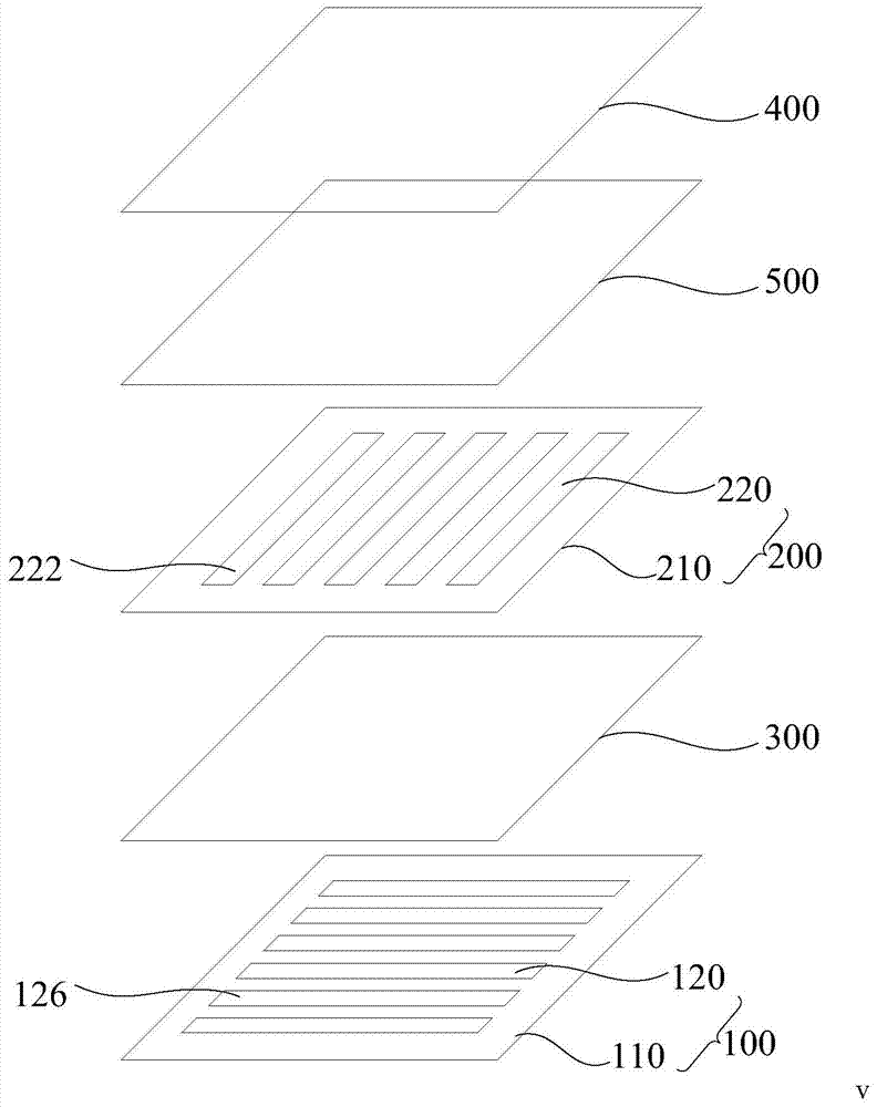
[0064] like figure 1 and figure 2 As shown, the touch screen 10 according to one embodiment includes a first touch substrate 100 , a second touch substrate 200 , a first transparent optical adhesive layer 300 , a protective panel 400 and a second transparent optical adhesive layer 500 .

[0065] The first touch control substrate 100 includes a first transparent substrate 110 and a first conductive layer 120 .

[0066] The material of the first transparent substrate 110 can be glass, polymethyl methacrylate, polycarbonate, polyethylene terephthalate, cycloolefin copolymer or cycloolefin polymer. The thickness of the first transparent substrate 110 is 0.02mm˜0.5mm. Further, in this embodiment, after comprehensively considering the processing difficulty of the first transp...


PUM

PropertyMeasurementUnit
thicknessaaaaaaaaaa
thicknessaaaaaaaaaa
thicknessaaaaaaaaaa

Abstract

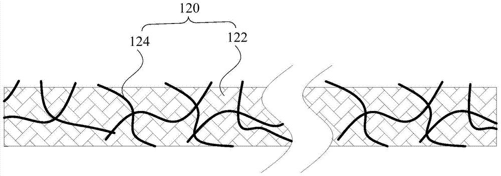
A touch control substrate, comprising: a transparent substrate; a conductive layer arranged on one side of the transparent substrate, the conductive layer includes a cured transparent photosensitive resin matrix and conductive nanowires embedded in the cured transparent photosensitive resin matrix, and the conductive nanowires are formed by cross connection Conductive grid; the conductive layer is patterned to form a plurality of touch electrodes. The above-mentioned touch substrate has good electrical conductivity. The invention also provides a manufacturing method of the touch substrate and a touch screen using the touch substrate.

Description

technical field [0001] The invention relates to the field of touch technology, in particular to a touch substrate, a manufacturing method thereof, and a touch screen using the touch substrate. Background technique [0002] A touch screen is an inductive device that receives touch input signals. The touch screen has endowed information interaction with a new look and is a very attractive new information interaction device. The development of touch screen technology has aroused widespread concern in the information media circles at home and abroad, and has become a rising high-tech industry in the optoelectronic industry. [0003] The touch screen includes a touch substrate and a protective panel laminated on the touch substrate. The traditional manufacturing method of touch substrate is usually as follows: [0004] (1) A conductive layer is formed directly on a transparent substrate. Taking an ITO (Indium Tin Oxide, indium tin oxide) conductive layer as an example, it is ...

Claims


Application Information

Patent Timeline
Patent Type & Authority Patents(China)
IPC IPC(8): G06F3/041
Inventor 唐根初刘伟蒋芳
Owner ANHUI JINGZHUO OPTICAL DISPLAY TECH CO LTD
Learn More