Negative Photosensitive Silicone Composition
A silane compound and photosensitivity technology, which is applied in optics, optomechanical equipment, instruments, etc., can solve the problem of transmittance decrease, and achieve the effect of excellent electrical insulation properties, high resolution, and high sensitivity
- Summary
- Abstract
- Description
- Claims
- Application Information
AI Technical Summary
Problems solved by technology
Method used
Image
Examples
Synthetic example 1
[0172]
[0173] In a 2L flask equipped with a stirrer, a thermometer, and a condenser, 36.5 g of a 25% by weight tetramethylammonium hydroxide aqueous solution, 300 ml of isopropanol (hereinafter referred to as IPA), and 1.5 g of water were mixed to prepare a reaction solvent. , and maintained at 10°C. Separately, a mixed solution of 44.6 g of phenyltrimethoxysilane, 34.1 g of methyltrimethoxysilane, and 3.8 g of tetramethoxysilane was prepared. This mixed solution was dripped at 10 degreeC using the dropping funnel in the reaction solvent, and after stirring for 2 hours maintaining at 10 degreeC, 10% HCl aqueous solution was added and neutralized. After adding and shaking 200 ml of toluene and 300 ml of water to the reaction liquid, it separated into two layers. The obtained organic layer was concentrated under reduced pressure to remove the solvent, and PGMEA was added to the concentrate to adjust the solid content to 40% by weight to prepare a solution containing polysil...
Embodiment 1
[0177]
[0178] Stirring was performed at the ratio of polysiloxane (Ia-1):(Ib-7)=(10% by weight): (90% by weight), and then the polysiloxane mixture was adjusted to a 35% by weight PGMEA solution. Measure the dissolution rate of this polysiloxane mixture to 2.38% TMAH aqueous solution after prebaking, the result is 105 / Second. To this siloxane mixture, 1.5% by weight of photoacid generator A1 (acid-releasing type) was added relative to the polysiloxane, and this photoacid generator A1 contained triphenylsulfonium cation and sulfonate anion, It can function by irradiating g-line or i-line. Moreover, 0.3 weight% of KF-53 (trade name, Shin-Etsu Chemical Co., Ltd. make) was added as surfactant with respect to polysiloxane, and the negative photosensitive silicone composition was obtained.
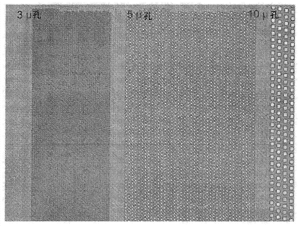
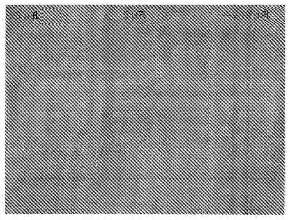
[0179] This photosensitive siloxane composition was applied to a silicon wafer by spin coating, and after application, it was prebaked on a hot plate at 100° C. for 90 seconds, and adjus...
Embodiment 2
[0180]
[0181] With respect to the polysiloxane mixture used in Example 1, the compounding ratio of the polysiloxane mixture was changed to polysiloxane (Ia-1): (Ib-8) = (10% by weight): (90 % by weight) to evaluate the dissolution rate of the polysiloxane mixture.
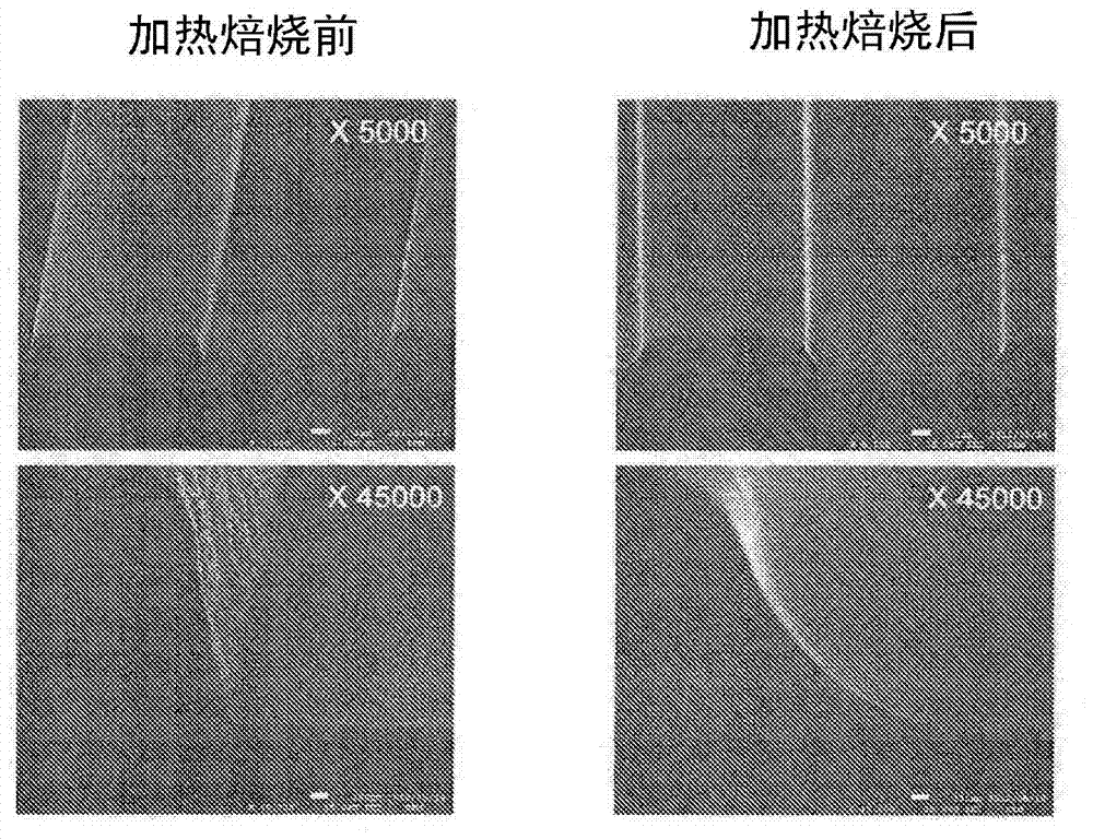
[0182] A negative photosensitive silicone composition was prepared in the same manner as in Example 1. This composition is coated on the substrate in the same manner as in Example 1, with 220mJ / cm 2 Exposure was performed to form a pattern, and as a result, it was confirmed that a line width / space pattern and a contact hole pattern of 8 μm were engraved in a state where no residue or the like was present. After forming the pattern, it was baked and solidified at 250° C., and it was confirmed by an optical microscope that a cylindrical 8 μm pattern was maintained.
PUM
| Property | Measurement | Unit |
|---|---|---|
| thermal resistance | aaaaa | aaaaa |
| transmittivity | aaaaa | aaaaa |
| relative permittivity | aaaaa | aaaaa |
Abstract
Description
Claims
Application Information
 - R&D
- Intellectual Property
- Life Sciences
- Materials
- Tech Scout
- Unparalleled Data Quality
- Higher Quality Content
- 60% Fewer Hallucinations
Browse by: Latest US Patents, China's latest patents, Technical Efficacy Thesaurus, Application Domain, Technology Topic, Popular Technical Reports.
© 2025 PatSnap. All rights reserved.Legal|Privacy policy|Modern Slavery Act Transparency Statement|Sitemap|About US| Contact US: help@patsnap.com


