PMOS (P-channel metal oxide semiconductor) transistor and forming method thereof

A technology of transistors and semiconductors, applied in the manufacture of transistors, semiconductor devices, semiconductor/solid-state devices, etc., can solve the problems of limited performance effect of PMOS transistors, difficulty in controlling the shape of sigma-shaped grooves, unstable performance of PMOS transistors, etc. Difficulty, shape is easier to control, and the effect of increasing compressive stress

Inactive Publication Date: 2014-06-18
SEMICON MFG INT (SHANGHAI) CORP
View PDF4 Cites 3 Cited by
  • Summary
  • Abstract
  • Description
  • Claims
  • Application Information

AI Technical Summary

Problems solved by technology

[0009] However, with the development of semiconductor technology, the requirements for device performance are getting higher and higher, and the existing PMOS transistor formation methods have limited effects in improving the performance of the formed PMOS transistor; The shape of the sigma-shaped groove formed by wet etching is difficult to control, and the performance of the formed PMOS transistor is unstable

Method used


Image

  • PMOS (P-channel metal oxide semiconductor) transistor and forming method thereof
  • PMOS (P-channel metal oxide semiconductor) transistor and forming method thereof
  • PMOS (P-channel metal oxide semiconductor) transistor and forming method thereof

Examples


Embodiment Construction

[0029] In order to make the above objects, features and advantages of the present invention more comprehensible, specific implementations of the present invention will be described in detail below in conjunction with the accompanying drawings.

[0030] In the following description, many specific details are set forth in order to fully understand the present invention, but the present invention can also be implemented in other ways than those described here, so the present invention is not limited by the specific embodiments disclosed below.

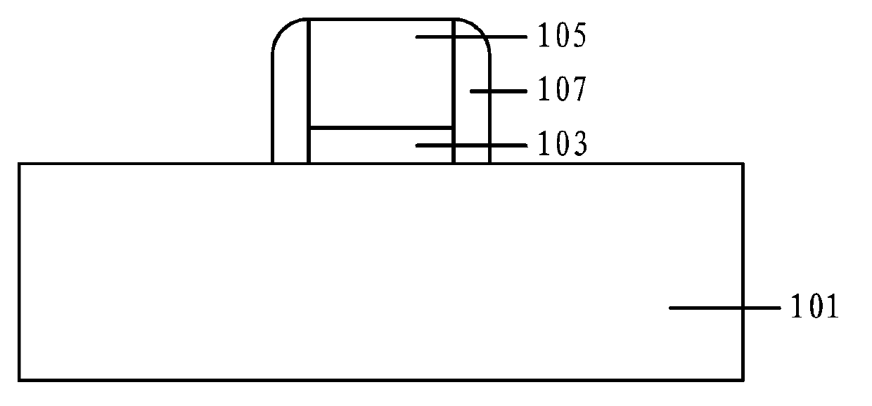
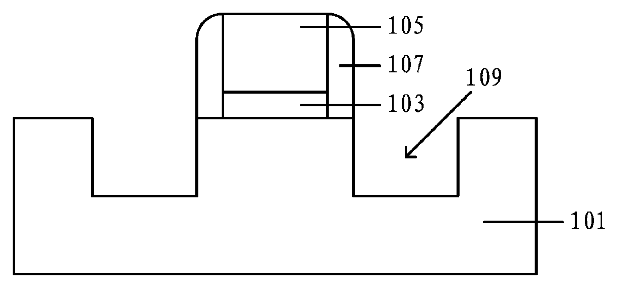
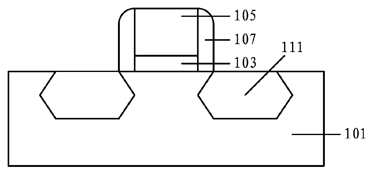
[0031] As mentioned in the background technology section, with the development of semiconductor technology, the requirements for device performance are getting higher and higher, and the existing PMOS transistor formation methods have limited effects in improving the performance of the formed PMOS transistor; The shape of the sigma-shaped groove formed by wet etching of the semiconductor substrate on the wall is difficult to control, and t...


PUM

PropertyMeasurementUnit
thicknessaaaaaaaaaa

Abstract

The invention provides a PMOS (P-channel metal oxide semiconductor) transistor and a forming method of the PMOS transistor. The PMOS transistor comprises a semiconductor substrate, a grid electrode structure, a main side wall and a germanium-silicon layer, wherein the grid electrode structure is positioned on the semiconductor substrate, the main side wall is positioned on the side wall of the grid electrode structure, the germanium-silicon layer is positioned in the semiconductor substrate positioned at the two sides of the main side wall, and the germanium-silicon is in a step shape with the gradually reduced line width. The forming method of the PMOS transistor has the advantages that the process is simple, and the performance of the formed PMOS transistor is better.

Description

technical field [0001] The invention relates to the technical field of semiconductor manufacturing, in particular to a PMOS transistor and a forming method thereof. Background technique [0002] As the most basic semiconductor device, transistors are currently being widely used. With the increase of component density and integration of semiconductor devices, the gate size of transistors has become shorter than before; however, the shortened gate size of transistors will make transistors The short channel effect is generated, and then leakage current is generated, which finally affects the electrical performance of the semiconductor device. At present, in the prior art, the stress of the channel region of the transistor is mainly increased to increase the mobility of carriers, thereby increasing the driving current of the transistor and reducing the leakage current in the transistor. [0003] In the prior art, the method for increasing the stress of the channel region of the...

Claims


Application Information

Patent Timeline
Patent Type & Authority Applications(China)
IPC IPC(8): H01L21/336H01L29/78H01L29/06
CPCH01L29/66568H01L29/7842
Inventor 张彬
Owner SEMICON MFG INT (SHANGHAI) CORP
Why Eureka
Try Eureka