Manufacturing method of capacitive touch screen

A technology of capacitive touch screen and manufacturing method, which is applied in the direction of electric digital data processing, instrument, input/output process of data processing, etc., can solve the problems that capacitive touch screen cannot meet the demand and cannot make curved surface, so as to prevent circuit breakage and improve Yield rate and the effect of avoiding disconnection failure

Inactive Publication Date: 2014-06-18
SHANTOU GOWORLD DISPLAY TECH CO LTD
View PDF6 Cites 1 Cited by
  • Summary
  • Abstract
  • Description
  • Claims
  • Application Information

AI Technical Summary

Problems solved by technology

However, in the current single-chip capacitive touch screen, the circuit layer needs to be processed on a flat panel by means of coating, photolithography, etc. Therefore, this kind of capacitive touch screen can only be designed as a plane, and cannot be made into a curved surface. As the designs of electronic products using touch screens, such as mobile phones and tablet computers, become more and more diverse, it is increasingly difficult for this flat capacitive touch screen to meet the needs of these electronic products.

Method used


Image

  • Manufacturing method of capacitive touch screen
  • Manufacturing method of capacitive touch screen
  • Manufacturing method of capacitive touch screen

Examples


Embodiment 1

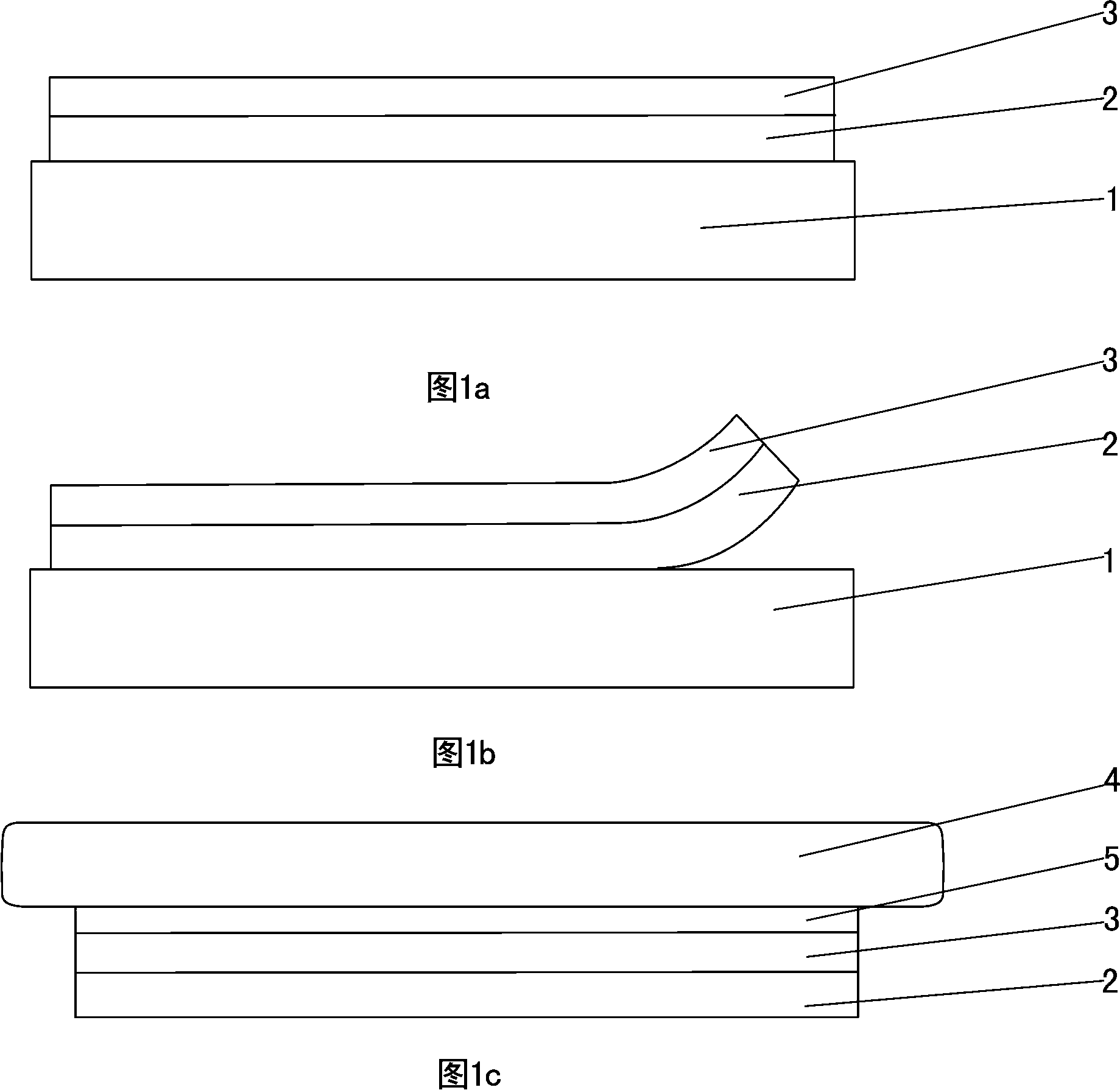
[0041] Such as figure 1 As shown, the manufacturing method of this capacitive touch screen includes the following steps:

[0042] (1) A circuit layer 2 with touch sensing function is formed on a motherboard 1;

[0043] (2) Coating and curing a polymer tough layer 3 on the circuit layer 2, the adhesive force of the tough layer 3 and the circuit layer 2 is greater than the bonding force of the circuit layer 3 and the motherboard 1;

[0044] (3) Separate the tough layer 3 from the motherboard 1, and the circuit layer 2 is adhered to the tough layer 3;

[0045] (4) The protective sheet 4 is adopted, and the first adhesive layer 5 is arranged on the protective sheet 4 (or the tough layer 3);

[0046] (5) Stick the flexible layer 3 on the protective sheet 4, so that the circuit layer 2 is closely attached to the protective sheet 4 through the flexible layer 3, the first adhesive layer 5, and the circuit layer 2, the protective sheet 4, and the flexible layer 3 together constitute a capacitor ...

Embodiment 2

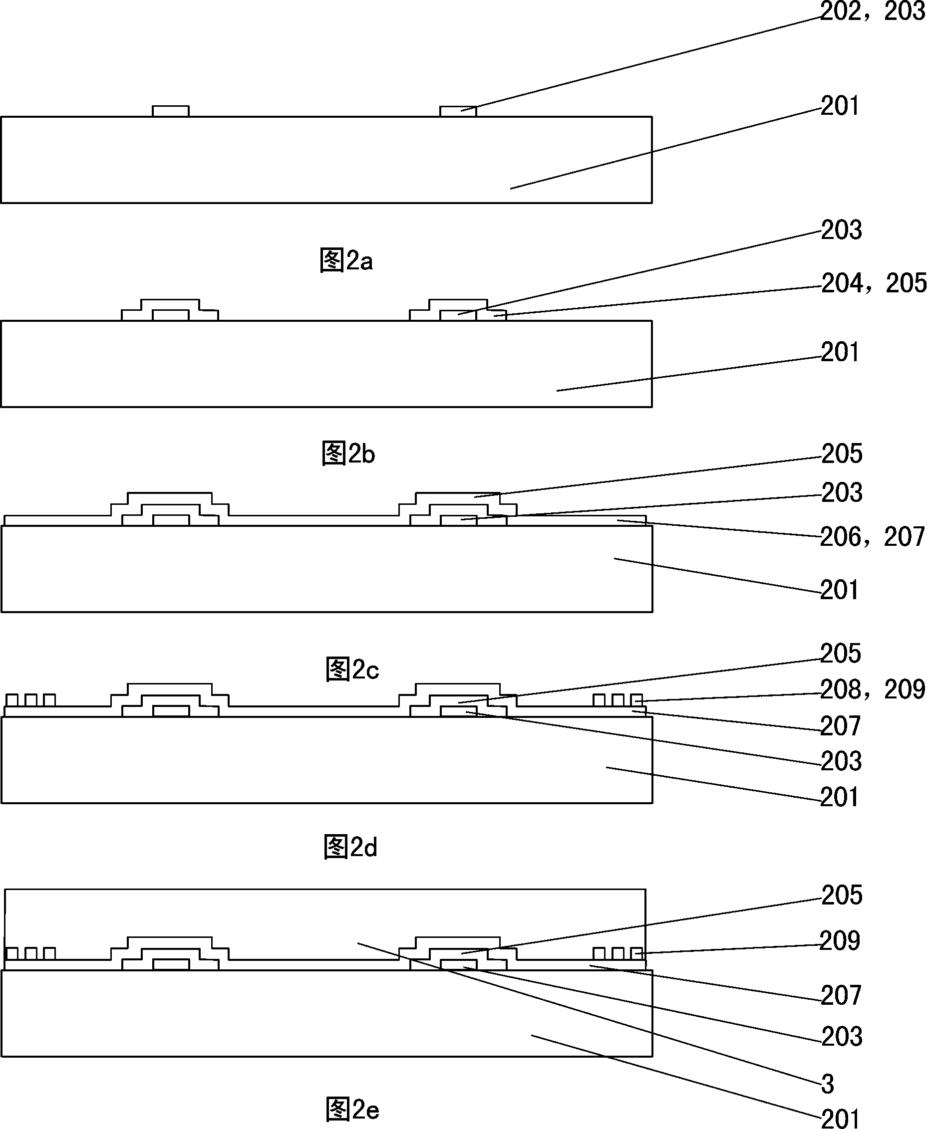
[0055] Such as Figure 5 As shown, when the other parts are the same as the first embodiment, the difference is that the production of the circuit layer includes the following steps:

[0056] (1) A first silver nanowire conductive film 202' is formed on the mother board 201' to form the first sensing electrode of the circuit layer 2'. The first silver nanowire conductive film 202' is made of linear nano silver in the glue Dispersed

[0057] (2) An insulating layer 204' is formed on the first silver nanowire conductive film 202';

[0058] (3) A second silver nanowire conductive film 206' is formed on the insulating layer 204' to form the first sensing electrode of the circuit layer 2'. The second silver nanowire conductive film 206' is made of linear nano silver in the glue Dispersed

[0059] (4) Fabricate the peripheral circuit layer 209'.

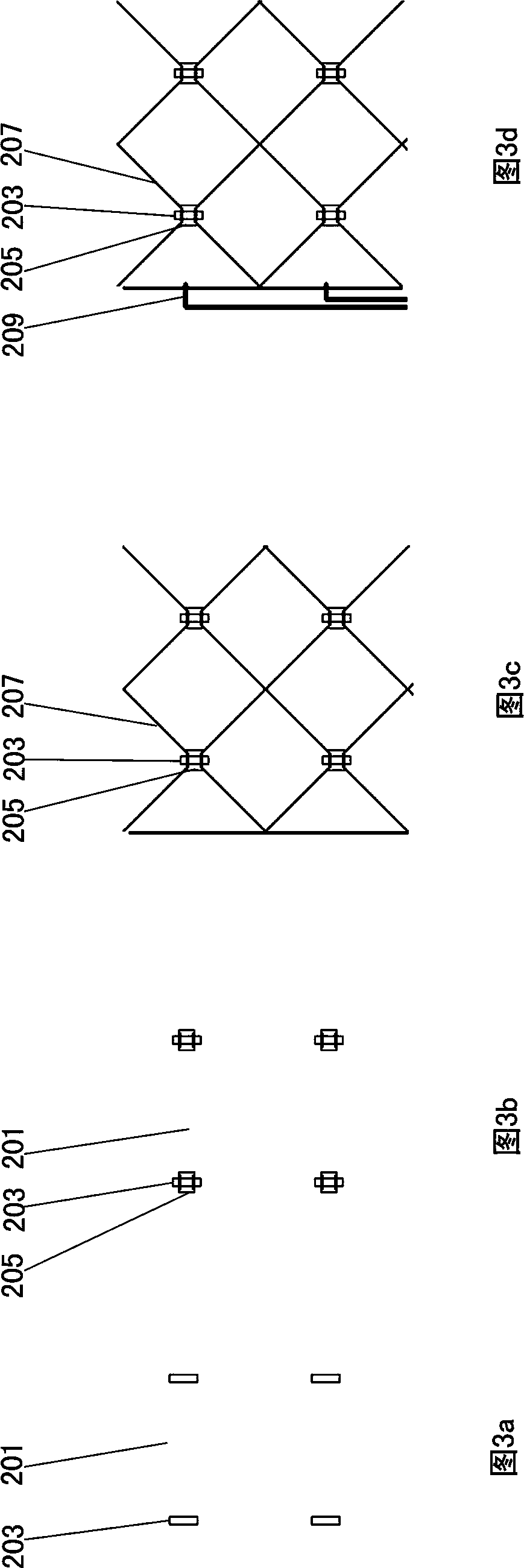
[0060] The capacitive touch screen manufactured by the above method is like Image 6 Shown.

Embodiment 3

[0062] Such as Figure 7 with Figure 8 As shown, when the other parts are the same as in the first or second embodiment, the difference is that the circuit layer includes a fingerprint scanning circuit, and the fingerprint scanning circuit includes a plurality of micro-patterned silver nanowire conductive films. The fingerprint detection matrix 11 formed by the electrodes 10, the size of each microelectrode 10 is less than 50μm, each microelectrode 10 contains a plurality of nano silver wires 12, and each nano silver wire 12 is randomly distributed. Both ends constitute a potential probe 13, and the potential probe 13 can detect the potential of the fingerprint based on the principle of capacitance.


PUM


Abstract

The invention relates to a manufacturing method of a capacitive touch screen, which comprises the following steps: a circuit layer with a touch sensitive function is formed on a mother board; a polymer ductile layer is coated on the circuit layer and the circuit layer and the ductile layer are solidified, and the adhesive force of the ductile layer and the circuit layer is greater than the binding force of the circuit layer and the mother board; the ductile layer is enabled to be separated from the mother board, and the circuit layer is adhered to the ductile layer; a first adhesive layer is arranged on a protection plate or the ductile layer; the ductile layer is adhered to the protection plate, and the circuit layer, the protection plate and the ductile layer form the capacitive touch screen. The circuit layer is transferred from the motor board through the ductile layer, and is finally adhered to the protection plate, and the ductile layer has a circuit layer connection effect and a circuit layer transfer effect. The breakage of the circuit layer is prevented, so that the line breakage fault during the separation process of the circuit layer and the mother board is avoided, the yield of the touch screen finished products is improved, the manufacturing cost is lowered, and the protection plate can adopt a plane or a curved surface, so that the capacitive touch screen can be made into a curved surface.

Description

Technical field [0001] The invention relates to the field of touch screen manufacturing, and in particular to a method for manufacturing a capacitive touch screen. Background technique [0002] The structure of the projected capacitive touch screen generally includes a circuit layer with capacitive touch sensing function and a protective sheet. The circuit layer generally includes a conductive film layer with a thickness of less than 1 μm such as a transparent conductive film and a metal film, which is arranged inside the protective sheet. When the finger touches the outside of the protective sheet, the circuit layer can detect the touch action of the finger through the capacitive sensing principle. [0003] At present, some people have proposed a single-chip capacitive touch screen structure. The circuit layer of the single-chip capacitive touch screen is directly fabricated on the inner surface of the protective sheet (such as strengthened glass lens). Therefore, the overall thic...

Claims


Application Information

Patent Timeline
Patent Type & Authority Applications(China)
IPC IPC(8): G06F3/0346
Inventor 沈奕吕岳敏林钢詹前贤崔卫星郑清交林伟浩欧建平
Owner SHANTOU GOWORLD DISPLAY TECH CO LTD
Why Eureka
Try Eureka