
Technology for producing 12-inch monocrystalline silicon epitaxial wafers through pressure reduction

An epitaxial wafer, single crystal silicon technology, applied in the direction of single crystal growth, single crystal growth, crystal growth, etc., can solve the problems affecting the application of silicon epitaxial wafer, etc., to reduce self-diffusion effect, uniform resistivity, improve resistivity The effect of distribution

Active Publication Date: 2014-05-28
GRINM SEMICONDUCTOR MATERIALS CO LTD
View PDF3 Cites 15 Cited by
  • Summary
  • Abstract
  • Description
  • Claims
  • Application Information

AI Technical Summary

Problems solved by technology

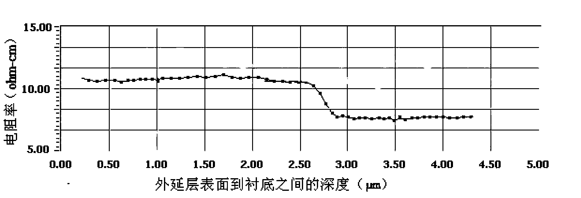
However, usually in the epitaxial process, due to the self-diffusion effect of the silicon wafer or the thermal diffusion effect of impurities inside the epitaxial furnace, the epitaxial layer and the surface resistivity transition zone of the silicon wafer are relatively wide, which affects the performance of the silicon epitaxial wafer in high-frequency devices, etc. field application

Method used


Image

  • Technology for producing 12-inch monocrystalline silicon epitaxial wafers through pressure reduction
  • Technology for producing 12-inch monocrystalline silicon epitaxial wafers through pressure reduction

Examples


Embodiment 1

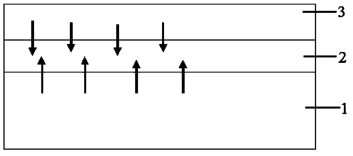
[0027] When preparing to produce epitaxial wafers, ensure that the gas required for epitaxy, water cooling and other peripheral services are normal, heat the reaction chamber to 900°C, heat up for 5 to 10 minutes, heat up to 1190°C, and feed high-purity HCl gas to clean the chamber The deposition layer inside the body and on the base, and then pass through the high-purity H with a large flow rate of 50SLM 2 Purge the residual HCl gas and reaction products inside the cavity to ensure that there are as few impurities as possible in the cavity, including dopants, so as not to affect the resistivity of the epitaxial layer.

[0028] After the reaction chamber is corroded by high-purity HCl gas, its temperature is lowered to 850°C, and the 12-inch monocrystalline silicon wafer is loaded onto the reaction base by a robot, and then the pressure in the reaction chamber is reduced to 80Torr by a vacuum pump, so that The 12-inch monocrystalline silicon wafer is in a decompressed environm...


PUM

PropertyMeasurementUnit
thicknessaaaaaaaaaa
thicknessaaaaaaaaaa

Abstract

The invention provides a technology for producing 12-inch monocrystalline silicon epitaxial wafers through pressure reduction. The technology comprises the following steps: (1) cleaning a reaction cavity with high-purity HCl gas at 1150-1190 DEG C; (2) introducing high-purity H2 to purge the HCl gas and reaction products remaining in the reaction cavity; (3) lowering the temperature inside the reaction cavity to 700-900 DEG C, loading 12-inch monocrystalline silicon wafers onto a slide glass base; (4) reducing the pressure intensity inside the reaction cavity to 20-200 Torr, then heating to 1000-1050 DEG C, wherein the flow rate of the carrier gas high-purity H2 is 40-160 SLM; (5) pre-flowing reaction gas, and adjusting the process and the time that DCS and doping agent are introduced into the reaction cavity to grow an epitaxial layer; (6) cooling to 900 DEG C, and taking out the epitaxial wafers. Through the technology provided by the invention, the epitaxial wafers which have the advantages that electrical resistivity of the epitaxial layer is uniform and the epitaxial layer and substrate electrical resistivity transition areas are narrow can be prepared.

Description

technical field [0001] The invention relates to a process for producing 12-inch monocrystalline silicon epitaxial wafers under reduced pressure. Background technique [0002] With the development of silicon semiconductor technology, the size of single crystal silicon wafers is required to be larger and larger, and the international market is gradually transitioning from 6 or 8 inch single crystal silicon wafers to 12 inch single crystal silicon wafers. Single crystal silicon wafers produced by the traditional Czochralski process have indispensable native defects, which will reduce the yield and reliability of subsequent devices. As the size of single crystal silicon wafers increases, it becomes more and more difficult to control the native defects of single crystal. [0003] Using the method of vacuum vapor deposition to grow the epitaxial layer has good crystal integrity, can eliminate surface or near-surface defects of silicon polished wafers, and improve the final chip y...

Claims


Application Information

Patent Timeline
Patent Type & Authority Applications(China)
IPC IPC(8): C30B25/16C30B29/06H01L21/205H01L21/02
Inventor 赵而敬冯泉林闫志瑞李宗峰盛方毓
Owner GRINM SEMICONDUCTOR MATERIALS CO LTD
Learn More