Physical Vapor Deposition Device

A physical vapor deposition and body technology, applied in the direction of ion implantation plating, metal material coating process, coating, etc., can solve the problems of reducing process quality, chamber particle pollution, and reducing service life, so as to improve performance stability, The effect of reducing the current resistance requirement and prolonging the life

Active Publication Date: 2016-08-31
BEIJING NAURA MICROELECTRONICS EQUIP CO LTD
View PDF4 Cites 0 Cited by
  • Summary
  • Abstract
  • Description
  • Claims
  • Application Information

AI Technical Summary

Problems solved by technology

These deposits can cause particle contamination of the chamber and reduce process quality when these deposits flake off
When the voltage difference is high, the Faraday shield will be bombarded by a large number of high-energy ions, causing sputtering, resulting in wear and reduced life

Method used


Image

  • Physical Vapor Deposition Device
  • Physical Vapor Deposition Device
  • Physical Vapor Deposition Device

Examples


Embodiment Construction

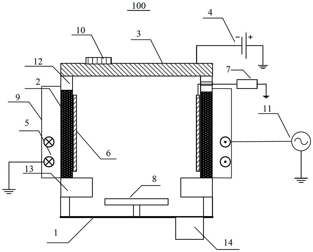
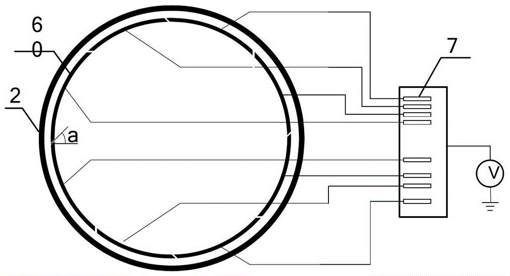
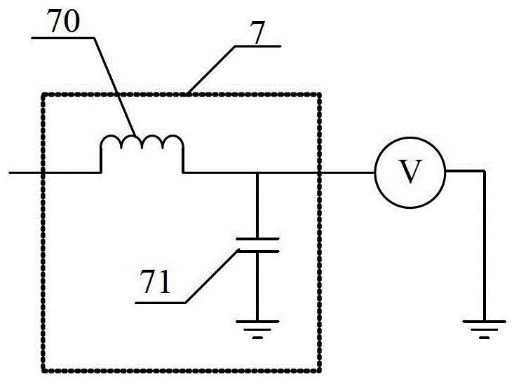
[0024] The embodiments of the present invention will be described in detail below. Examples of the embodiments are shown in the accompanying drawings, wherein the same or similar reference numerals indicate the same or similar elements or elements with the same or similar functions. The embodiments described below with reference to the drawings are exemplary, and are only used to explain the present invention, but should not be understood as limiting the present invention.

[0025] In the description of the present invention, it should be understood that the terms "center", "upper", "lower", "front", "rear", "left", "right", "vertical", "horizontal", The orientation or positional relationship indicated by "top", "bottom", "inner", "outer", etc. is based on the orientation or positional relationship shown in the drawings, and is only for the convenience of describing the present invention and simplifying the description, and does not indicate or imply The device or element referre...


PUM


Abstract

The invention discloses a physical vapor deposition device, which comprises a chamber body, a radio frequency coil, a faraday shielding element, a plurality of unsymmetrical pressure regulation units and a base, wherein a dielectric cylinder and a target arranged at the top of the dielectric cylinder are arranged in the chamber body; the target is connected with a direct current power supply; the radio frequency coil is arranged in the chamber body, and is arranged on the outer side of the dielectric cylinder in a sleeving manner to excite process gas introduced into the chamber body into plasmas; the faraday shielding element is arranged on the inner wall of the dielectric cylinder, and comprises a plurality of shielding fragments which are distributed along the circumferential direction of the dielectric cylinder at intervals; the shielding fragments are connected to the unsymmetrical pressure regulation units in a one-to-one correspondence way, so that unsymmetrical pressure values of the shielding fragments are regulated respectively; the base is arranged in the chamber body, and is used for placing a chip to be processed. According to the physical vapor deposition device, the etching rate and deposition rate of the faraday shielding element are substantially equal, so that the probability of pollution to a chamber can be reduced, and the service life of the faraday shielding element can also be prolonged.

Description

Technical field [0001] The invention relates to the field of physical vapor deposition, in particular to a physical vapor deposition device. Background technique [0002] Physical vapor deposition (PVD) technology or sputtering (Sputtering) deposition technology is the most widely used type of thin film manufacturing technology in the semiconductor industry. It generally refers to the thin film preparation process that uses physical methods to prepare thin films. The ionization rate of metal atoms is a key indicator of this technology. [0003] The coil inductive coupling method can excite high-density plasma. Because there is usually a large change in the RF voltage on the coil, there is a capacitive coupling between the coil and the generated plasma. This capacitive coupling will reduce the plasma discharge efficiency and increase the bombardment of the plasma on the dielectric wall. . In order to reduce this capacitive coupling, a Faraday shield is usually used between the di...

Claims


Application Information

Patent Timeline
Patent Type & Authority Patents(China)
IPC IPC(8): C23C14/34
Inventor 吕铀
Owner BEIJING NAURA MICROELECTRONICS EQUIP CO LTD
Why Eureka
Try Eureka