Formation method of electrical interconnection structure

It is a technology of electrical interconnection and conductive structure, which is applied in the manufacture of circuits, electrical components, semiconductors/solid-state devices, etc. It can solve problems such as poor stability and poor copper interconnection structure morphology, achieve stable performance, avoid damage, and simplify The effect of craft

Active Publication Date: 2016-04-20
SEMICON MFG INT (SHANGHAI) CORP
View PDF5 Cites 0 Cited by
  • Summary
  • Abstract
  • Description
  • Claims
  • Application Information

AI Technical Summary

Problems solved by technology

[0008] However, the copper interconnect structure formed by the existing technology has poor morphology and poor stability

Method used


Image

  • Formation method of electrical interconnection structure
  • Formation method of electrical interconnection structure
  • Formation method of electrical interconnection structure

Examples


no. 1 example

[0042] Such as Figure 4 to Figure 8 Shown is a schematic cross-sectional structure diagram of the method for forming the electrical interconnection structure described in the first embodiment of the present invention.

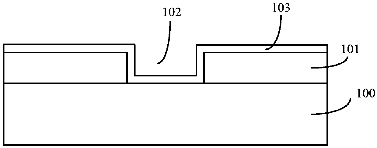
[0043] Please refer to Figure 4 , provide a semiconductor substrate 300, the surface of the semiconductor substrate 300 has a dielectric layer 301, the dielectric layer 301 has a first opening 302 through its thickness.

[0044] The semiconductor substrate 300 is used to provide a working platform for subsequent processes; the semiconductor substrate 300 is a silicon substrate, a silicon-germanium substrate, a silicon carbide substrate, a silicon-on-insulator (SOI) substrate, a germanium-on-insulator (GOI) substrate, or a silicon-on-insulator (GOI) substrate. ) substrate, glass substrate or III-V compound substrate (such as silicon nitride or gallium arsenide, etc.).

[0045] There is a conductive layer 310 in the semiconductor substrate 300, the surface of...

no. 2 example

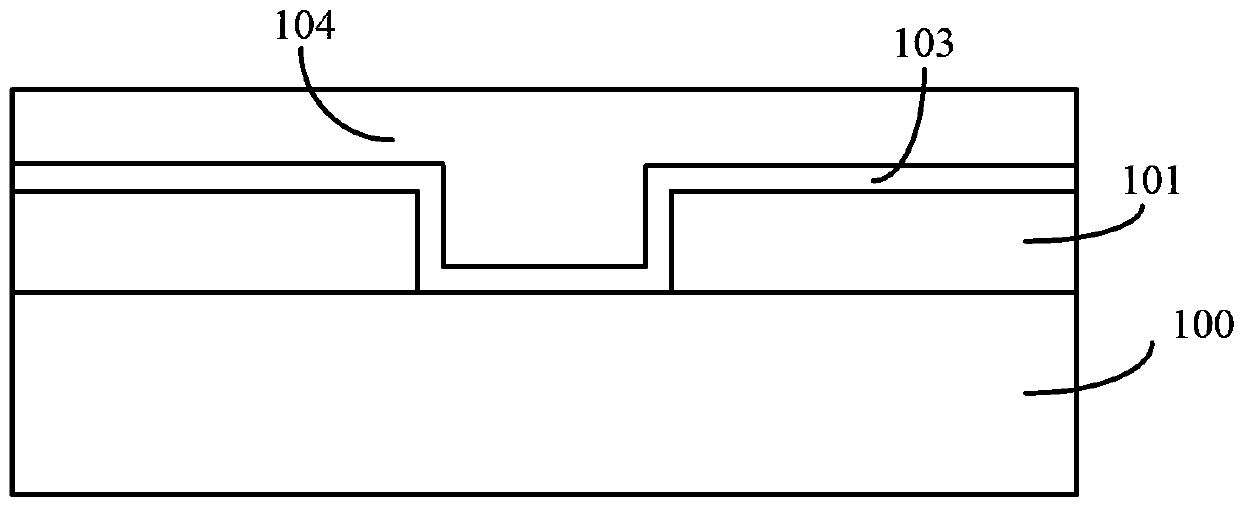
[0067] Such as Figure 9 to Figure 12 Shown is a schematic cross-sectional structure diagram of the method for forming the electrical interconnection structure described in the second embodiment of the present invention.

[0068] Please refer to Figure 9 , provide a semiconductor substrate 200, the surface of the semiconductor substrate 200 has a dielectric layer 201, the dielectric layer 201 has a first opening 202 through its thickness; on the surface of the dielectric layer 201 and the first opening 202 The sidewalls and bottom surface form the seed layer 203 .

[0069] The semiconductor substrate 200 , the dielectric layer 201 , the first opening 202 , the conductive layer 210 and the seed layer 203 are as described in the first embodiment, and will not be repeated here.

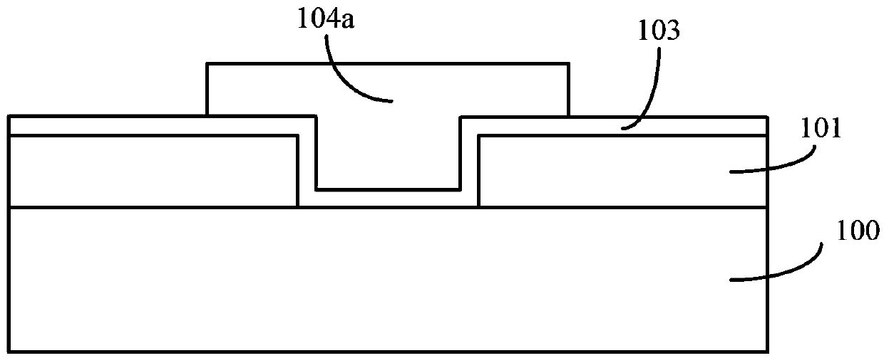
[0070] Please refer to Figure 10 , forming a first photoresist layer 204 on the surface of the seed layer 203, the material of the first photoresist layer 204 is a non-conductive photoresist, and th...


PUM


Abstract

A formation method for an electrical interconnection structure comprises the following steps: providing a dielectric layer on the surface of a semiconductor substrate, wherein the dielectric layer is internally provided with a first opening running through the thickness of the dielectric layer; forming a seed layer on the surface of the dielectric layer and the side walls and the bottom surface of the first opening; forming a second photoresist layer on the seed layer, wherein the material of the second photoresist layer is conductive photoresist, and the second photoresist layer is internally provided with a third opening running through the thickness of the second photoresist layer, the bottom of the third opening exposing the first opening; forming a first photoresist layer on the surface of the second photoresist layer, wherein the material of the first photoresist layer is non-conductive photoresist, and the first photoresist layer is internally provided with a second opening running through the thickness of the first photoresist layer, the second opening being communicated with the third opening; utilizing an electroplating process to form a conductive structure on the surface of the seed layer in the first opening and the bottom of the third opening, wherein the top surface of the conductive structure is lower than or equal to the top surface of the first photoresist layer; and after the conductive structure is formed, removing the second photoresist layer and the first photoresist layer. The electrical interconnection structure is stable in performance.

Description

technical field [0001] The invention relates to the technical field of semiconductor manufacturing, in particular to a method for forming an electrical interconnection structure. Background technique [0002] In the field of semiconductor manufacturing, in order to realize the electrical connection between semiconductor devices, various metal interconnect structures and forming processes have been developed, such as copper interconnect structures, and copper electroplating processes (ECP, electro -copperingplating). However, with the development of ultra-large-scale integration (ULSI), the feature size (CD) of semiconductor devices is continuously reduced, and the process of forming metal interconnection structures is also challenged. [0003] Schematic diagram of the cross-sectional structure of the formation process of the copper interconnection structure in the prior art, such as Figure 1 to Figure 3 shown, including: [0004] Please refer to figure 1 , forming a die...

Claims


Application Information

Patent Timeline
Patent Type & Authority Patents(China)
IPC IPC(8): H01L21/768
CPCH01L21/76877H01L21/76879
Inventor 洪中山
Owner SEMICON MFG INT (SHANGHAI) CORP
Why Eureka
Try Eureka