Fine line preparation method

A line and fine technology, which is applied in the field of electron beam lithography and fine line preparation, can solve the problems of complex fine lines and increase process complexity, and achieve the effects of reducing roughness, improving stability, and reducing fluctuations

Active Publication Date: 2014-05-07
INST OF MICROELECTRONICS CHINESE ACAD OF SCI
View PDF8 Cites 4 Cited by
  • Summary
  • Abstract
  • Description
  • Claims
  • Application Information

AI Technical Summary

Problems solved by technology

[0004] On the other hand, using traditional optical exposure technology to prepare fine lines such as polysilicon gate electrodes is complicated. In order to obtain 22nm-level l

Method used


Image

  • Fine line preparation method
  • Fine line preparation method
  • Fine line preparation method

Examples


Embodiment Construction

[0020] The features and technical effects of the technical solution of the present invention will be described in detail below with reference to the accompanying drawings and in combination with exemplary embodiments. It should be pointed out that similar reference numerals represent similar structures, and the terms "first", "second", "upper", "lower", "thick", "thin" and the like used in this application can be used for Modify various device structures. These modifications do not imply a spatial, sequential or hierarchical relationship of the modified device structures unless specifically stated.

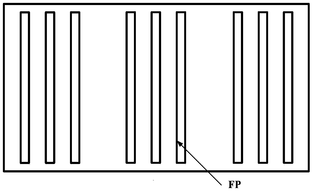
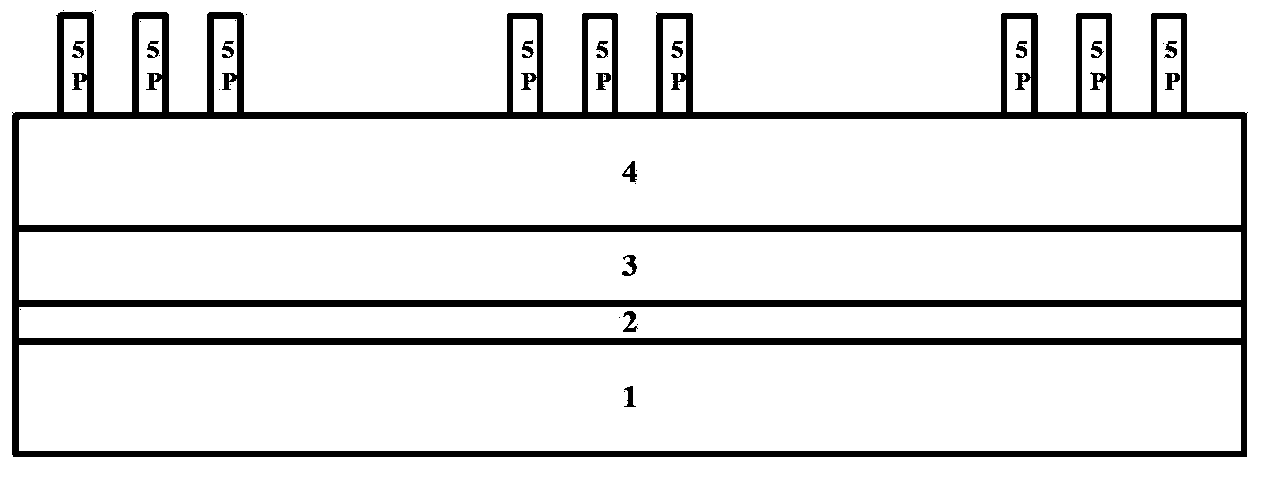
[0021] Reference attached figure 1 , shows a schematic diagram of an e-beam lithography layout for small linewidth features such as gate electrode layers, local interconnect layers, etc. In the present invention, the fine pattern FP is defined as a pattern that is beyond the capability of ordinary optical exposure and needs to be exposed by electron beams, and lines with a patte...


PUM


Abstract

The invention discloses a fine line preparation method which comprises the steps of forming a structural material layer and hard mask layers on a substrate, forming electron beam photoresist on the hard mask layers and performing electron beam exposure to form an electron beam photoresist pattern, carrying out etching with the use of the electron beam photoresist pattern as a mask to form a hard mask pattern, and etching the structural material layer with the use of the hard mask pattern as a mask to form a needed fine line. According to the method of the invention, a plurality of hard mask layers of different materials are adopted and etching reaction conditions are reasonably adjusted, the roughness of the side wall of the electron beam photoresist is prevented from being transferred to the lower structural material layer, the line roughness is effectively reduced, the process stability is improved, and the fluctuation of device performance is reduced.

Description

technical field [0001] The invention relates to the field of semiconductor integrated circuit manufacturing, and more specifically, to an electron beam lithography and a method for preparing fine lines. Background technique [0002] With the gradual reduction of VLSI feature size, the technical limit of ordinary optical exposure has come after entering the 22nm technology generation in the manufacturing method of semiconductor devices. At present, after the 45nm process node, i193nm immersion lithography technology combined with double exposure and double etching technology is generally used to prepare smaller lines. Fine patterning at nodes below 22nm typically requires exposure and lithography using e-beam or EUV. [0003] Regarding EUV lithography technology, it is still in the research and development stage, and there are still several key technologies that need to be overcome and improved, and it cannot be applied to large-scale integrated circuit manufacturing. In co...

Claims


Application Information

Patent Timeline
IPC IPC(8): H01L21/033G03F1/80
CPCH01L21/0332H01L21/32139
Inventor 孟令款李春龙贺晓彬
Owner INST OF MICROELECTRONICS CHINESE ACAD OF SCI
Why Eureka
Try Eureka