Method for manufacturing thin film transistor substrate

A technology of thin film transistors and manufacturing methods, which is applied in the field of liquid crystal display, can solve problems such as deterioration, destruction, and instability of oxide semiconductor thin film transistors, and achieve the effects of avoiding crowding effects, reducing production costs, and improving quality

Active Publication Date: 2014-04-16
TCL CHINA STAR OPTOELECTRONICS TECH CO LTD
View PDF5 Cites 12 Cited by
  • Summary
  • Abstract
  • Description
  • Claims
  • Application Information

AI Technical Summary

Problems solved by technology

[0008] Although the oxide semiconductor thin film transistor with the back channel structure has a simple structure and process, and has a high channel width-to-length ratio (W / L), the etching process of the metal source / drain electrode 200' usually uses strong acid and its mixture. (such as HNO 3 / H 3 PO 4 / CH 3 COOH, etc.) as an etchant, the oxide semiconductor layer 100' at the back channel is easily damaged, resulting in deterioration and instability of the characteristics of the oxide semiconductor thin film transistor

Method used


Image

  • Method for manufacturing thin film transistor substrate
  • Method for manufacturing thin film transistor substrate
  • Method for manufacturing thin film transistor substrate

Examples


Embodiment Construction

[0036] In order to further illustrate the technical means adopted by the present invention and its effects, the following describes in detail in conjunction with preferred embodiments of the present invention and accompanying drawings.

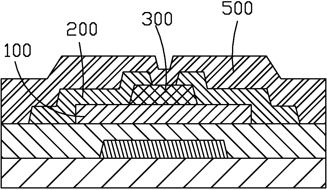
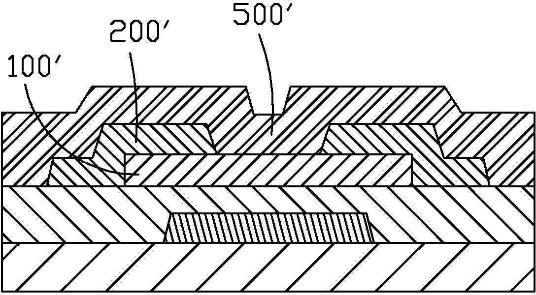
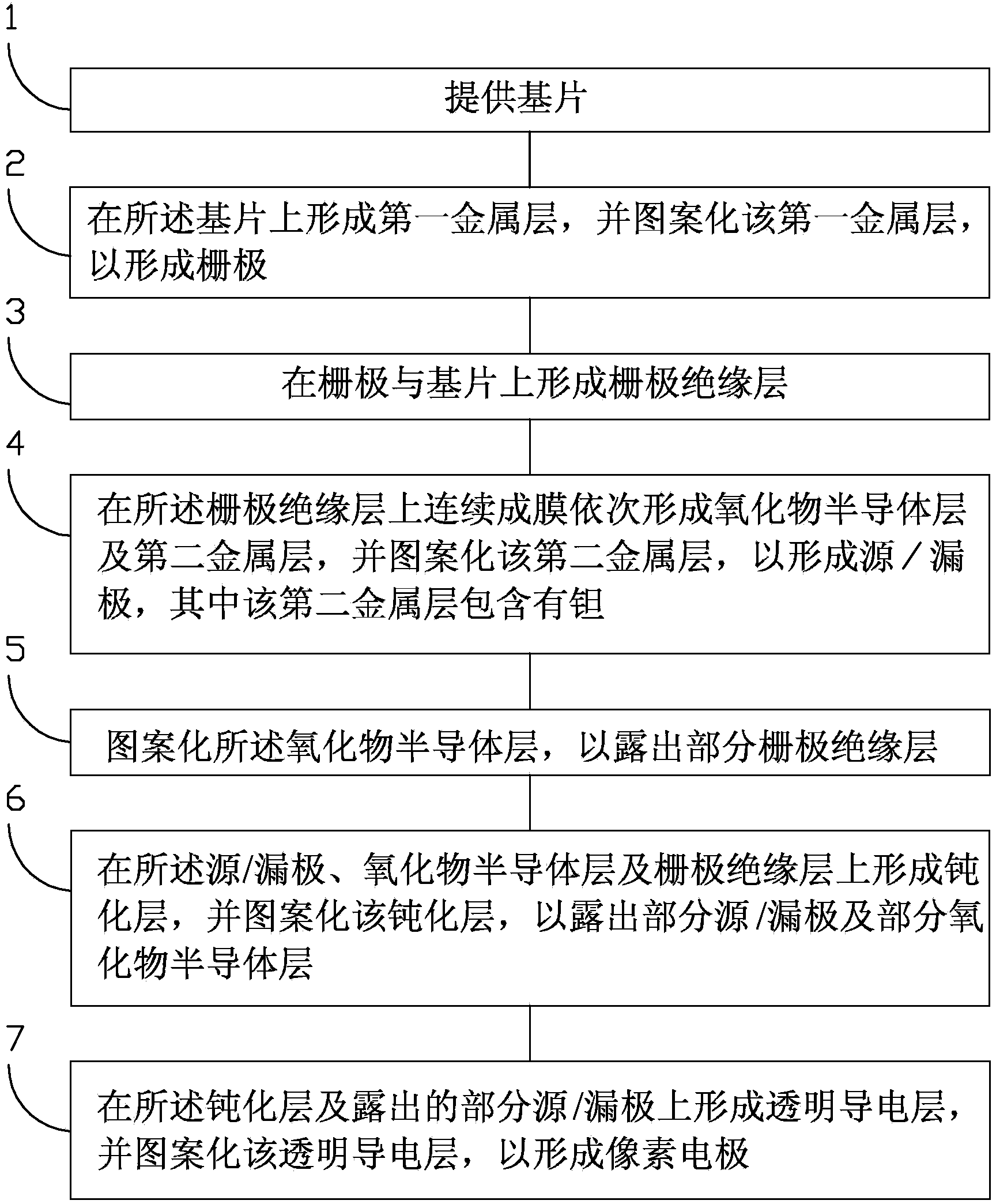
[0037] see image 3 , and refer to Figure 4 to Figure 9 , the invention provides a method for manufacturing a thin film transistor substrate, comprising the following steps:

[0038] Step 1, providing a substrate 20 .

[0039] The substrate 20 is a transparent substrate, preferably a glass substrate or a plastic substrate. In this embodiment, the substrate 20 is a glass substrate.

[0040] Step 2, forming a first metal layer on the substrate 20 and patterning the first metal layer to form the gate 22 .

[0041] Specifically, the first metal layer is formed by deposition on the substrate 20 , and then the first metal layer is exposed, developed and etched through a mask or a half mask to form a grid 22 with a predetermined pattern. The fir...


PUM


Abstract

The invention provides a method for manufacturing a thin film transistor substrate. According to the method, the manufacture procedure is simple, a good contact interface is achieved through a continuous film forming oxide semiconductor layer and a source / drain electrode, and the crowding effect due to the fact that contact resistance is too large is avoided. Meanwhile, the source / drain electrode is made of metal materials containing tantalum, an etching solution containing hydrogen peroxide is used for etching the source / drain electrode in the etching manufacturing process, damage of a traditional etching solution to the oxide semiconductor layer is avoided, and the quality of the thin film transistor substrate is improved. Moreover, an etching blocking layer does not need to be additionally manufactured to protect the oxide semiconductor layer on a back channel, the high width to length ratio (W / L) of the channel is guaranteed, the structure of the thin film transistor substrate is simplified, the manufacturing procedures are reduced, production cost is lowered, and the yield rate is improved.

Description

technical field [0001] The invention relates to the field of liquid crystal display, in particular to a manufacturing method of a thin film transistor substrate. Background technique [0002] Thin film transistors (TFTs) are widely used in electronic devices as switching devices and driving devices. In particular, thin film transistors are commonly used in the field of flat panel display devices such as liquid crystal display devices (LCD), organic light emitting display devices (OLED), electrophoretic display devices (EPD), etc., because they can be formed on glass substrates or plastic substrates. [0003] Due to the high electron mobility of oxide semiconductors (mobility of oxide semiconductors>10cm 2 / Vs, the mobility of amorphous silicon (a-Si) is only 0.5-0.8cm 2 / Vs), and compared with low-temperature polysilicon (LTPS), the oxide semiconductor process is simpler and has higher compatibility with the amorphous silicon process, and can be applied to liquid crysta...

Claims


Application Information

Patent Timeline
Patent Type & Authority Applications(China)
IPC IPC(8): H01L21/77
CPCH01L29/66969H01L27/1225H01L29/7869H01L27/127
Inventor 胡哲陈宇霆詹润泽董承远江政隆陈柏林赖梓杰
Owner TCL CHINA STAR OPTOELECTRONICS TECH CO LTD
Why Eureka
Try Eureka