Drain/source region dielectric (pn junction) isolation front gate n-mosfet radio frequency switch ultra-low loss device based on soi process

A drain region and front gate technology, applied in semiconductor devices, electrical components, circuits, etc., can solve problems such as large loss, high on-state power consumption, unfavorable device and overall system performance, and achieve the effect of reducing loss

Active Publication Date: 2016-09-28
HANGZHOU DIANZI UNIV
View PDF5 Cites 0 Cited by
  • Summary
  • Abstract
  • Description
  • Claims
  • Application Information

AI Technical Summary

Problems solved by technology

When the SOI N-MOSFET device works normally, the channel formed by the conduction of source and drain is only on the top surface of the P-type channel region, and it is a lateral channel, and the gate field plate covers the gate oxide layer, resulting in the on-state work High power consumption, low working efficiency of the device, large loss when used as a radio frequency switch, which is not conducive to improving the overall performance of the device and system

Method used


Image

  • Drain/source region dielectric (pn junction) isolation front gate n-mosfet radio frequency switch ultra-low loss device based on soi process
  • Drain/source region dielectric (pn junction) isolation front gate n-mosfet radio frequency switch ultra-low loss device based on soi process

Examples


Embodiment Construction

[0015] The present invention will be further described below in conjunction with the accompanying drawings and specific embodiments.

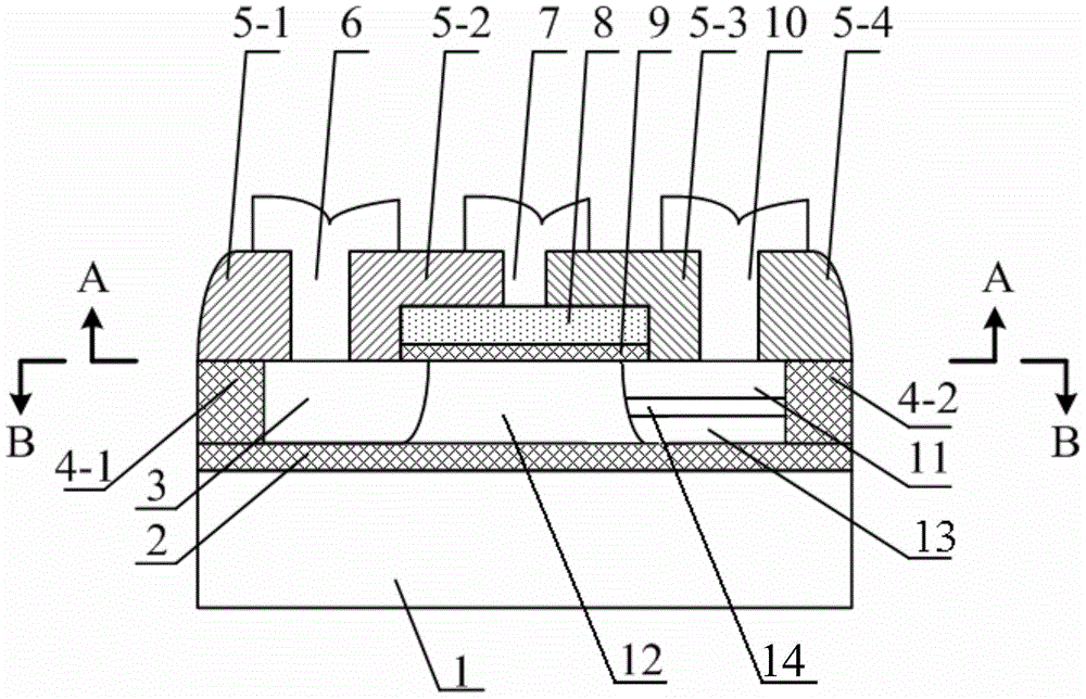
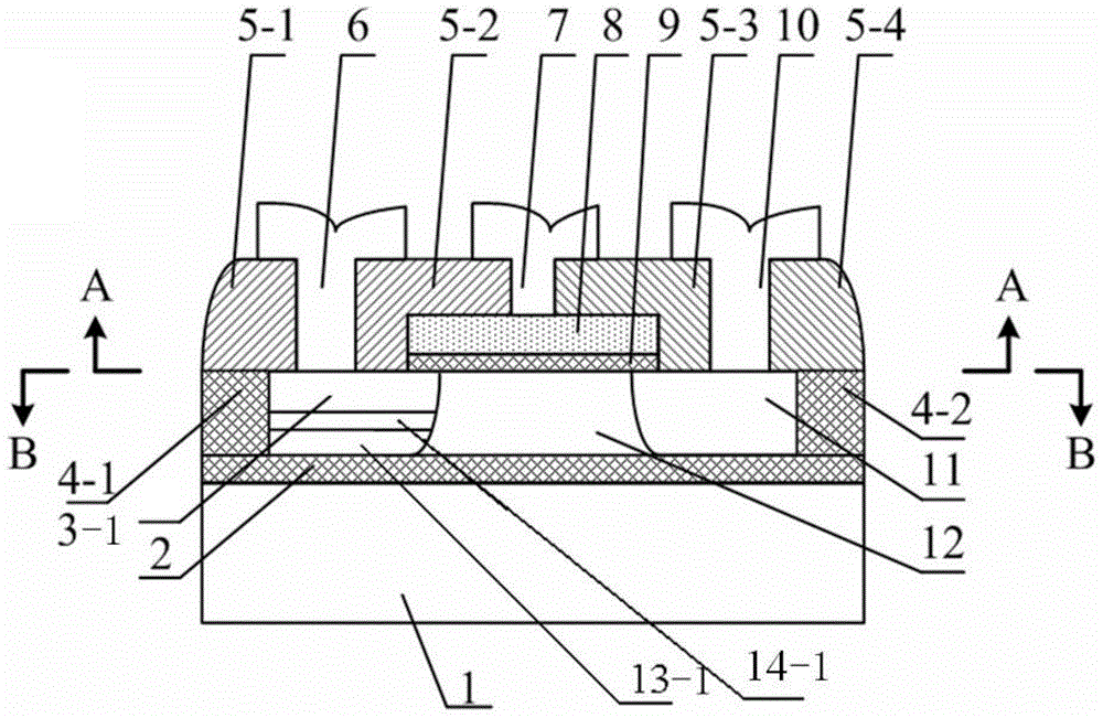
[0016] Such as figure 1 As shown, the drain region dielectric / PN junction isolation front gate N-MOSFET radio frequency switch ultra-low loss device based on SOI process includes P-type semiconductor substrate 1, buried oxide layer 2, P-type channel region 12, and N-type source region 3. The N-type drain region 11 of the front gate MOSFET, the N-type drain region 13 of the back gate MOSFET, the N-type drain region isolation region 14 and the deep trench isolation region (4-1, 4-2); the buried oxide layer 2 covers On the P-type semiconductor substrate 1, the P-type channel region 12 is arranged on the buried oxide layer 2, and the deep trench isolation regions (4-1, 4-2) are arranged on the buried oxide layer 2 and surround the P-type channel Region 12, N-type source region 3, N-type drain region 11 of the front gate MOSFET, N-type drain region...


PUM


Abstract

The invention discloses a drain / source region medium (PN junction) isolation front grid N-MOSFET (Metal-Oxide-Semiconductor Field Effect Transistor) radio frequency switch ultralow loss device based on a SOI (Silicon on Insulator) process. A SOIN-MOSFET device source (drain) region is remoulded, a PN junction or a dielectric capacitance is formed on the source (drain) region, the junction depth of the source region is deeper, a P-type doping or medium is manufactured in the middle of the drain region to form the PN junction or the dielectric capacitance, and the isolation of direct current bias applied to the drain region is formed; through the arrangement of body grid and back grid bias, a back grid MOSFET channel is on, and a drain region alternating current signal of a front grid N-MOSFET is coupled to a back grid MOSFET; as the back grid MOSFET works in an on state, the structure adjusts the impedance under the on state of the front grid MOSFET, the radio frequency loss when the front grid N-MOSFET is used for switch on-state application is reduced, and the loss of the radio frequency switch is ultralow; when a self-heating effect of the device is produced and causes the back grid MOSFET to form negative impedance, or when the back grid MOSFET works in an amplification state, a front grid coupling signal can be directly amplified, the energy loss under the front grid on-state is compensated, and the loss is further reduced.

Description

technical field [0001] The invention belongs to the field of semiconductor technology, and relates to an ultra-low loss radio frequency switch of a drain (source) region dielectric (PN junction) isolation front gate N-MOSFET (N-type metal-oxide-semiconductor transistor) based on a semiconductor process on an SOI insulating layer device. Background technique [0002] The SOI N-MOSFET device eliminates the latch-up effect due to the dielectric isolation, and its unique insulating buried layer structure greatly reduces the parasitic effect of the device, greatly improves the performance of the circuit, and has small parasitic capacitance and integrated With the advantages of high density, fast speed, simple process, and small short channel effect, it is widely used in low voltage, low power consumption, high speed, radiation resistance, high temperature resistance and other fields. The structure of a conventional SOI N-MOSFET device is a sandwich structure of an insulating sub...

Claims


Application Information

Patent Timeline
Patent Type & Authority Patents(China)
IPC IPC(8): H01L29/78H01L29/06
CPCH01L29/0873H01L29/0882H01L29/7831
Inventor 刘军
Owner HANGZHOU DIANZI UNIV
Why Eureka
Try Eureka