
A method for improving the uniformity of n-type doping concentration in a silicon carbide epitaxial wafer

A technology of doping concentration and epitaxial wafers, which is applied in chemical instruments and methods, crystal growth, electrical components, etc., can solve problems such as background concentration, surface morphology defect density changes, difficulties, etc., and achieve excellent background concentration and doping concentration Uniformity optimization, the effect of enlarging the selection window

Active Publication Date: 2016-03-16
NO 55 INST CHINA ELECTRONIC SCI & TECHNOLOGYGROUP CO LTD
View PDF2 Cites 0 Cited by
  • Summary
  • Abstract
  • Description
  • Claims
  • Application Information

AI Technical Summary

Problems solved by technology

However, changes in such parameters will also bring about changes in important indicators of epitaxial wafers such as background concentration, surface morphology, and defect density.
Finding a suitable process window is very difficult

Method used


Image

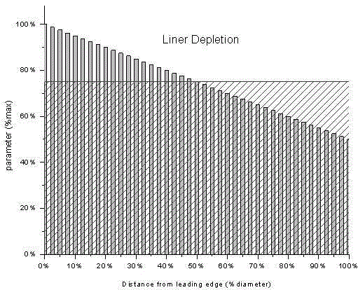
  • A method for improving the uniformity of n-type doping concentration in a silicon carbide epitaxial wafer
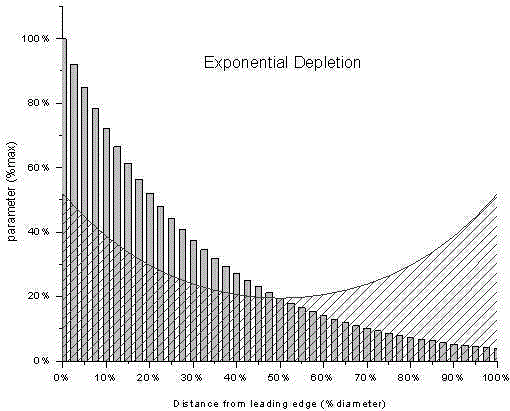
  • A method for improving the uniformity of n-type doping concentration in a silicon carbide epitaxial wafer
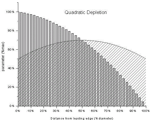
  • A method for improving the uniformity of n-type doping concentration in a silicon carbide epitaxial wafer

Examples


Embodiment

[0037] The provided method for epitaxially growing a high-uniformity epitaxial material on a 100mm silicon surface 4H crystal silicon carbide substrate with a 4° bias to the direction includes the following steps:

[0038] 1) Select a 100mm silicon surface 4H crystal silicon carbide substrate with a 4° bias to the direction, and place the substrate on a graphite base coated with tantalum carbide;

[0039] 2) The temperature of the system is raised to 1400°C, the set pressure is 100mbar, and argon air flotation (air flotation flow rate 1000sccm) is selected, and in-situ hydrogen etching is performed on the substrate surface in an atmosphere of hydrogen gas (flow rate 80slm) to remove the surface of the substrate. damage and contamination, and inhibit the formation of steps, the treatment time is 30 minutes;

[0040] 3) The temperature of the system is raised to 1550°C. When the temperature is stabilized at 1550°C, silane (64sccm), propane (32sccm), hydrogen chloride (128sccm)...


PUM


Abstract

The invention relates to a method for increasing the uniformity of on-chip n-type doping concentration of a silicon carbide epitaxial wafer. According to the method, a chemical vapor deposition growth technology serves as basis; a silicon surface silicon carbide substrate with the deviation (11-20) direction of 4 degrees or 8 degrees is adopted; silane and propane serve as growth sources; hydrogen chloride serves as an auxiliary gas for inhibiting gas phase nucleation of a silicon component; hydrogen serves as a carrier gas and a diluent gas; nitrogen serves as an n-type doping agent. A small amount of process gas silane or propane is added into a base air floatation gas and is pushed by the air floatation gas serving as a carrier gas to the edge of the substrate to finely adjust the carbon silicon ratio of the edge of the substrate, so that the doping efficiency of the n-type doping source on the edge of the substrate is changed, the doping concentration deviation of the edge point and the central point of the epitaxial wafer caused by non-linear exhausting is effectively reduced, and the uniformity of the on-chip doping concentration of the epitaxial wafer is effectively optimized on the premise of not changing key process parameters. The selection window of the key process parameters is enlarged and technical support is provided for the growth of a high-quality silicon carbide epitaxial material.

Description

technical field [0001] The present invention proposes a method for improving the uniformity of the n-type doping concentration in the silicon carbide epitaxial wafer, which improves the uniformity of the doping concentration in the silicon carbide epitaxial wafer and reduces the The doping concentration deviation of the center point and the edge point of the SiC epitaxial wafer is calculated. It belongs to the technical field of semiconductor materials. Background technique [0002] Silicon carbide (SiC) devices are characterized by high temperature resistance, energy saving, and system miniaturization, making them widely used in the fields of PFC power supplies, air conditioners and other white goods, hybrid and pure electric vehicles, motor control, solar and wind power generation, railway transportation, and smart grids. Applications. [0003] The thickness and doping concentration uniformity of silicon carbide epitaxial materials seriously affect the performance of sil...

Claims


Application Information

Patent Timeline
Patent Type & Authority Patents(China)
IPC IPC(8): C30B33/12H01L21/02C30B29/36
Inventor 李赟
Owner NO 55 INST CHINA ELECTRONIC SCI & TECHNOLOGYGROUP CO LTD
Learn More