Negative-electrode active material, and method for production of negative-electrode active material
A technology of active materials and negative electrodes, applied in the field of preparation of negative electrode active materials, can solve the problems of low initial charge and discharge efficiency, improve charge and discharge efficiency and discharge capacity, and prevent irreversible reactions
- Summary
- Abstract
- Description
- Claims
- Application Information
AI Technical Summary
Problems solved by technology
Method used
Image
Examples
preparation example Construction
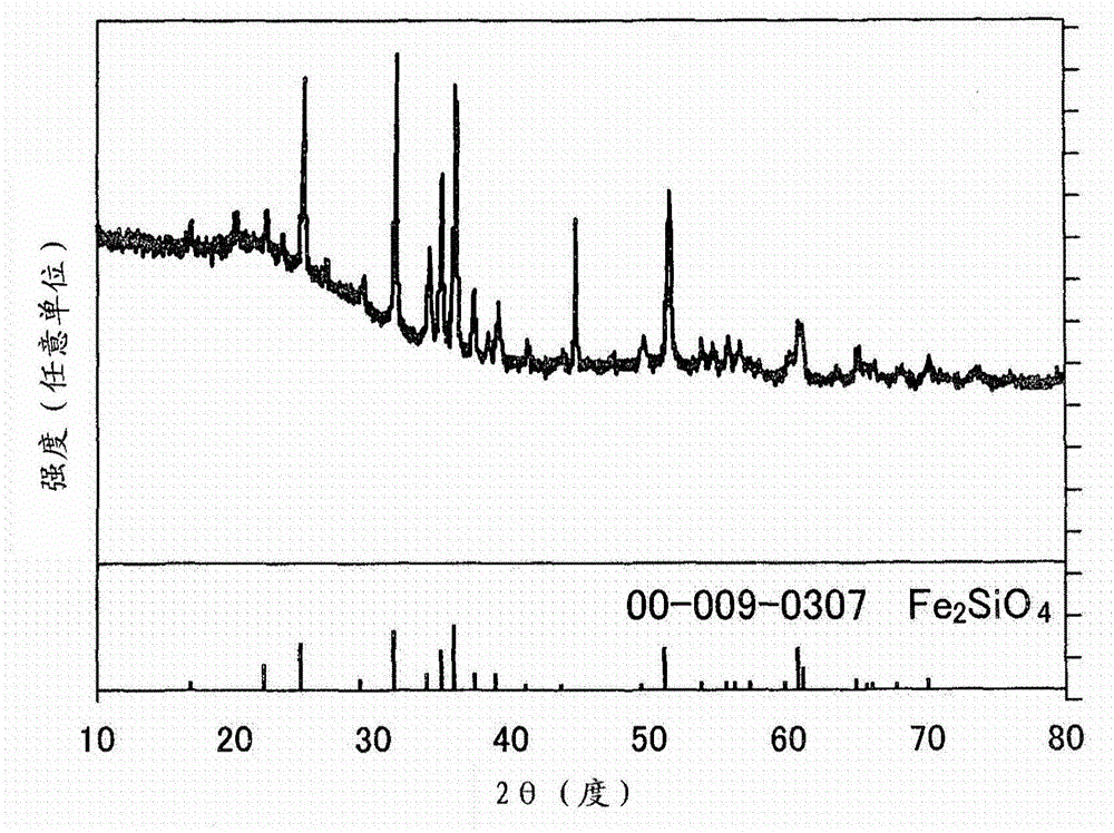
[0056] The preparation method of the negative electrode active material of the present invention is not particularly limited. Examples of methods include physically mixing silicon oxide SiO x Chemically mix silicon oxide SiO with silicate compound (1) and heat treatment x Mixed with silicate compounds (1) and electrochemically mixed silicon oxide SiO x With silicate compound (1). It is preferable to use the preparation method of the negative electrode active material of the present embodiment described below.
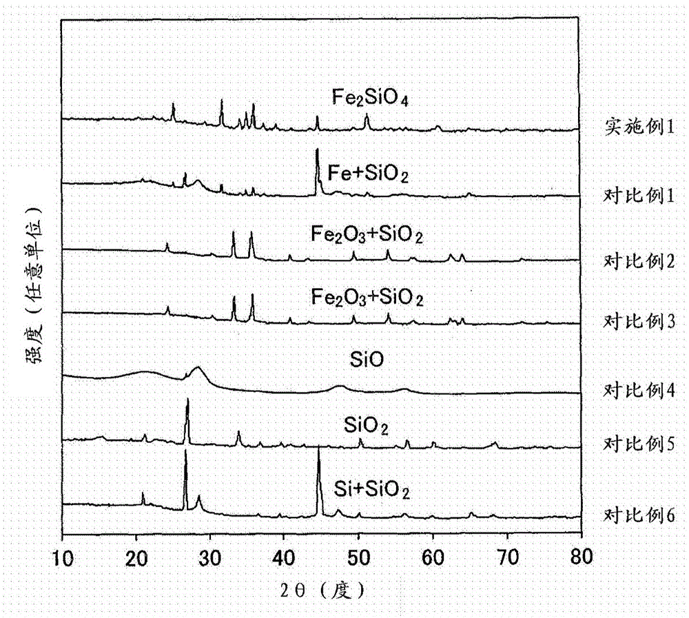
[0057] [Preparation method of negative electrode active material] The preparation method of the negative electrode active material of the present embodiment includes mixing SiO y (0<y<2) represents the mixing step of silicon oxide and metal oxide and the heat treatment step of heat-treating the mixture obtained in the mixing step in a non-oxidizing atmosphere. The negative absolute value of the standard Gibbs energy of the oxidation reaction of the metal oxide at the heati...
Embodiment 3
[0107] (Example 3) A negative electrode active material was obtained in the same manner as in Example 2, except that the reaction temperature was changed to 700°C.
Embodiment 4
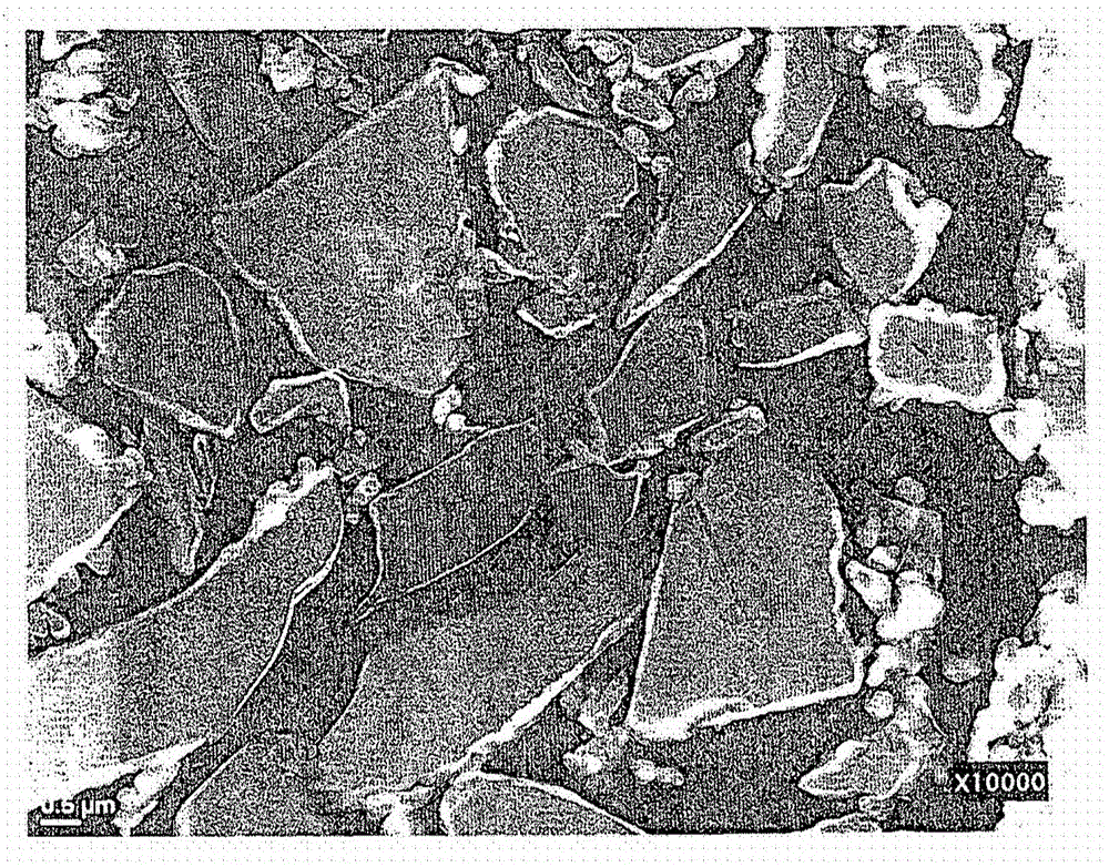
[0108] (Example 4) A negative electrode active material was obtained in the same manner as in Example 2, except that the reaction temperature was changed to 800°C. The form of the negative electrode active material was observed under a scanning transmission electron microscope (STEM). Figure 3 to Figure 5 A dark field STEM image (DF-STEM) is shown in. The gray area is SiO, the white area is Fe 2 SiO 4 . STEM observation and energy dispersive X-ray spectrometry (EXD) were performed on this negative electrode active material to observe the distribution of O, Si, and Fe. The results are shown in Figure 6A to 6D in. Figure 6A It is a DF-STEM image. Figure 6B The whitish area shows the distribution of O (oxygen), Figure 6C The whitish area shows the distribution of Si (silicon), Figure 6D The whitish area shows the distribution of Fe. The image in Fig. 6 indicates the presence of Fe compounds on the surface of the SiO phase. Figure 3 to Figure 6D The image in shows that in ...
PUM
| Property | Measurement | Unit |
|---|---|---|
| diameter | aaaaa | aaaaa |
| particle diameter | aaaaa | aaaaa |
| particle diameter | aaaaa | aaaaa |
Abstract
Description
Claims
Application Information
 - Generate Ideas
- Intellectual Property
- Life Sciences
- Materials
- Tech Scout
- Unparalleled Data Quality
- Higher Quality Content
- 60% Fewer Hallucinations
Browse by: Latest US Patents, China's latest patents, Technical Efficacy Thesaurus, Application Domain, Technology Topic, Popular Technical Reports.
© 2025 PatSnap. All rights reserved.Legal|Privacy policy|Modern Slavery Act Transparency Statement|Sitemap|About US| Contact US: help@patsnap.com


