Cyclic Etching Method of Silicon Nitride High Aspect Ratio Holes
A high aspect ratio, silicon nitride technology, used in electrical components, circuits, semiconductor/solid-state device manufacturing, etc., can solve the problems of difficult to control hole size, low selection ratio, etching stop, etc., to achieve the effect of rapid etching
- Summary
- Abstract
- Description
- Claims
- Application Information
AI Technical Summary
Problems solved by technology
Method used
Image
Examples
Embodiment 1
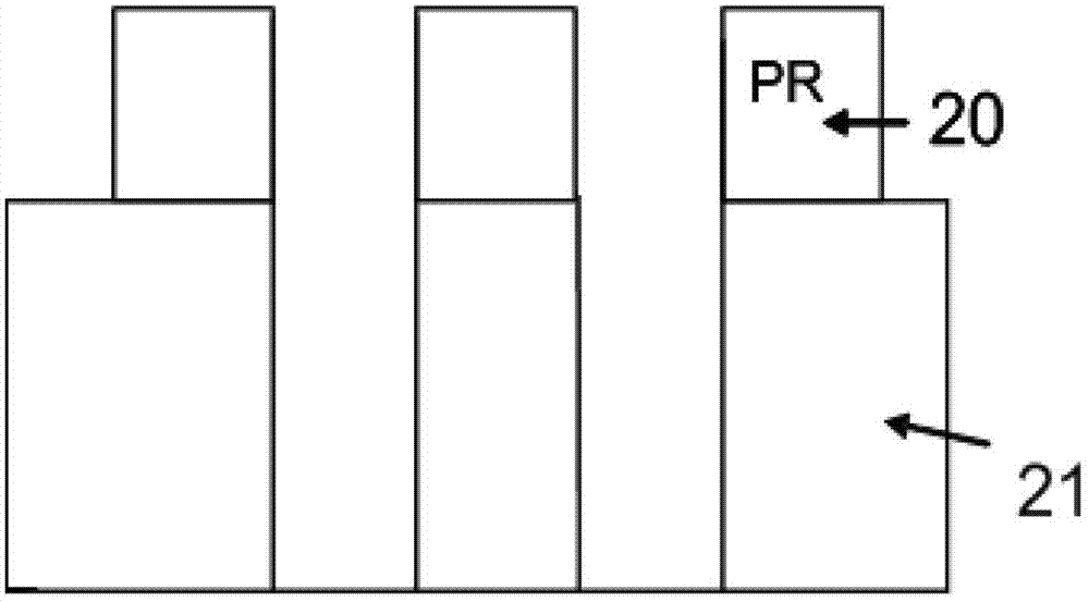
[0038] Embodiment 1. Etching a high-aspect-ratio hole with a steep shape on a single-layer silicon nitride film
[0039] image 3 It is a cross-sectional view of a steep etch topography of a high aspect ratio hole in a single-layer silicon nitride film according to Embodiment 1 of the present invention. In this embodiment, a layer of silicon nitride film 21 is firstly deposited on the substrate on which the basic semiconductor structure has been formed, and a photoresist is used as the mask 20 (depending on the requirements of different process nodes, sometimes it may be necessary to add a hard mask touch), photolithography out of the desired pattern. Then, an etching gas is introduced into the etching chamber, excited by radio frequency power, and after the plasma is stabilized, the two-step silicon nitride etching process of the present invention is performed.
[0040] In the first embodiment, firstly, the fluorocarbon-based etching gas CH is introduced in the first step. ...
Embodiment 2
[0043] Example 2: Etching a slightly inclined high-aspect-ratio hole on a single-layer silicon nitride film
[0044] Figure 4 It is a cross-sectional view of the slightly inclined etching topography of the high aspect ratio hole of the single-layer silicon nitride film according to the second embodiment of the present invention. Because for etched holes with high aspect ratio, figure 2 The steep topography shown poses considerable challenges for subsequent filling. Sometimes for the subsequent process, it is necessary to make the size of the bottom smaller to make a slightly inclined result. Embodiment 2 is also first to use PECVD to deposit a layer of silicon nitride film 31 on the substrate on which the basic semiconductor structure has been formed, and use photoresist as the mask 30 (depending on the requirements of different process nodes, sometimes it may be necessary to add a hard film). mask), photoetching out the desired pattern. Then, an etching gas is introduce...
Embodiment 3
[0047] Embodiment 3: Etching a high aspect ratio hole on a multilayer silicon nitride film
[0048] Figure 5 The etching cross-sectional view of the high aspect ratio hole of the multilayer silicon nitride film according to the third embodiment of the present invention. Embodiment 3 Firstly, a layer of silicon nitride film 41 is deposited on the surface of the device on which a multilayer semiconductor structure has been formed, and a photoresist is used as the mask 40 (depending on the requirements of different process nodes, sometimes it may be necessary to add a hard film). mask), photoetching out the desired pattern. Then, an etching gas is introduced into the etching chamber, excited by radio frequency power, and after the plasma is stabilized, a two-step silicon nitride etching process is performed.
[0049] The process parameters can refer to the above examples. It can stop above or below the dielectric layer 42 as desired. The difference between this embodiment an...
PUM
 Abstract
Description
Claims
Application Information
 - R&D
- Intellectual Property
- Life Sciences
- Materials
- Tech Scout
- Unparalleled Data Quality
- Higher Quality Content
- 60% Fewer Hallucinations
Browse by: Latest US Patents, China's latest patents, Technical Efficacy Thesaurus, Application Domain, Technology Topic, Popular Technical Reports.
© 2025 PatSnap. All rights reserved.Legal|Privacy policy|Modern Slavery Act Transparency Statement|Sitemap|About US| Contact US: help@patsnap.com


