Thin film thermocouple for metal cutting temperature measurement and manufacturing method thereof
A metal cutting and thermocouple technology, applied in the manufacture/processing of thermoelectric devices, measuring heat, and using electrical devices, etc., can solve the problem of difficult to meet the real-time acquisition of the transient temperature of the tool surface during cutting, many microscopic defects in the film, and difficult to shoot Problems such as the rake face, to achieve rapid dynamic response, short response time, and firm combination
- Summary
- Abstract
- Description
- Claims
- Application Information
AI Technical Summary
Problems solved by technology
Method used
Image
Examples
preparation example Construction
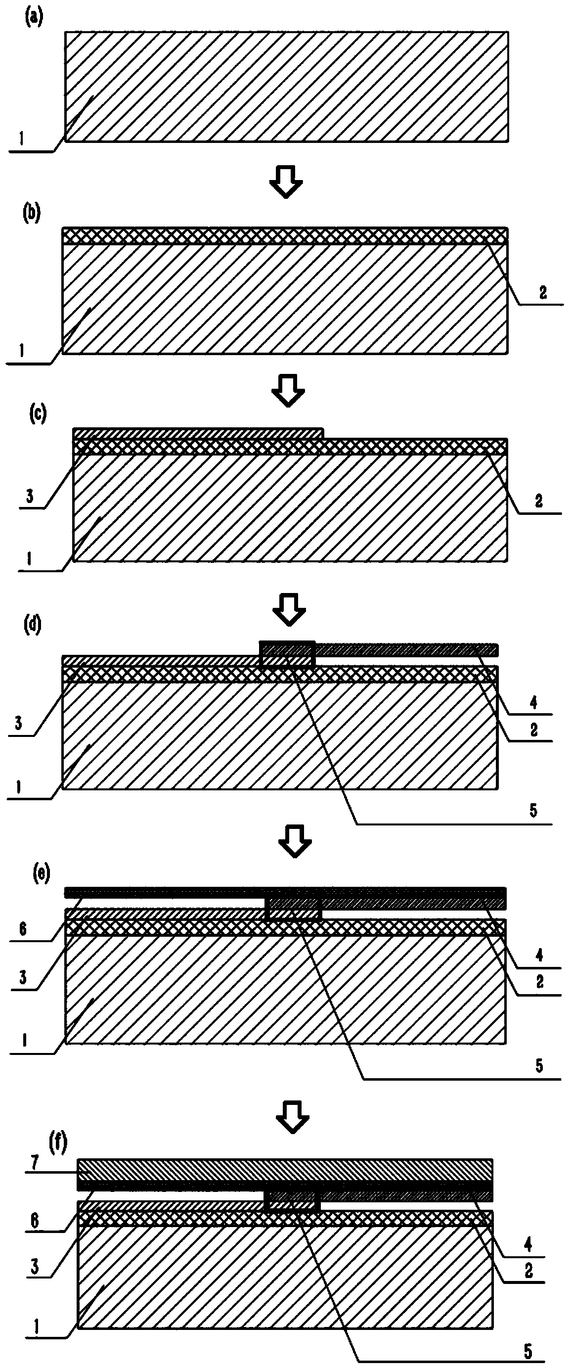
[0028] The preparation method of the thin-film thermocouple for metal cutting temperature measurement provided by the invention comprises the following steps (such as image 3 shown):
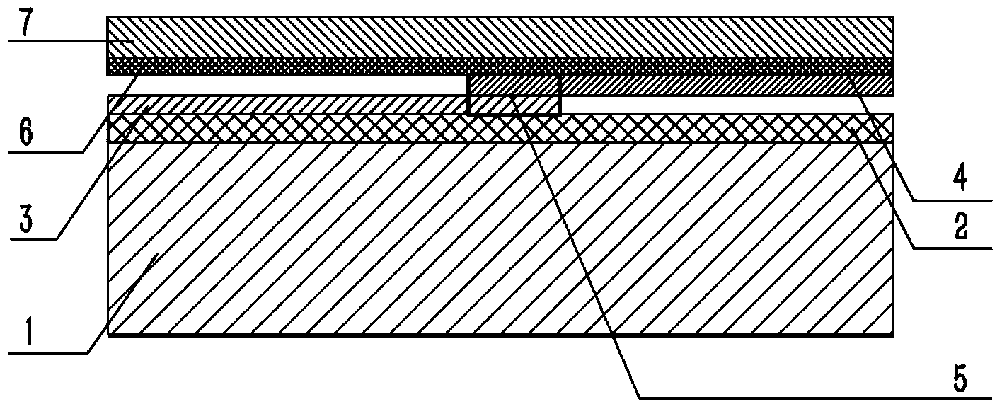
[0029] a) Deposit a layer of SiO with a thickness of 450-550nm on the surface of the ceramic turning tool blade 2 , forming a buffer layer 2, the surface roughness is controlled within the range of 25±5nm;
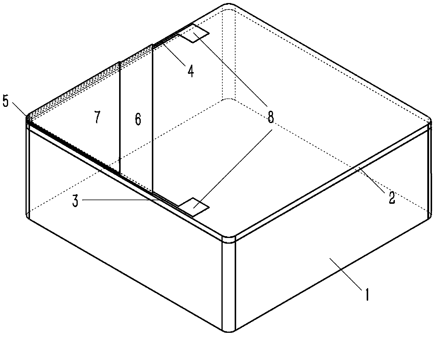
[0030] b) Using two hollow mechanical masks made of high-temperature-resistant molybdenum, the Ni electrode 3 with a thickness of 100-150 nm and the NiCr electrode 4 with the same thickness were prepared on the buffer layer by using an electron beam evaporation coating platform; the Ni electrode and the NiCr electrode Form a temperature measuring hot node 5 at the tip of the knife; and set an electrode terminal board 8 at the ends of the two electrodes;
[0031] c) Put the thin-film thermocouple prepared in step b) into a resistance furnace, and keep it warm for 28-30 minutes at a tempera...
Embodiment
[0035] Embodiment: The specific dimensions of the thin-film thermocouple in this embodiment are shown in Table 1.
[0036] Table 1. Dimensional design of specific examples of thin-film thermocouples
[0037]
[0038] In a specific embodiment of the invention, its processing steps are:
[0039] a) in Al 2 o 3 A layer of SiO is deposited on the surface of ceramic turning tool insert substrate 1 2 Buffer layer 2, with a thickness of 500nm, aims to improve the problem of excessive roughness of the substrate (relative to the thin film coating), and control the surface roughness of the substrate within the range of 25±5nm;
[0040] b) A hollow mechanical mask made of high temperature resistant molybdenum material ( Figure 4 ), it is very stable at high temperature, and hardly diffuses with the thermocouple electrode film, which greatly improves the purity of the electrode. The size of the mask plate is consistent with the base of the turning tool blade, which can achieve a c...
PUM
| Property | Measurement | Unit |
|---|---|---|
| Area | aaaaa | aaaaa |
| Thickness | aaaaa | aaaaa |
| Thickness | aaaaa | aaaaa |
Abstract
Description
Claims
Application Information
 - R&D Engineer
- R&D Manager
- IP Professional
- Industry Leading Data Capabilities
- Powerful AI technology
- Patent DNA Extraction
Browse by: Latest US Patents, China's latest patents, Technical Efficacy Thesaurus, Application Domain, Technology Topic, Popular Technical Reports.
© 2024 PatSnap. All rights reserved.Legal|Privacy policy|Modern Slavery Act Transparency Statement|Sitemap|About US| Contact US: help@patsnap.com


