Production method of graphene field-effect transistor

A technology of field effect transistor and manufacturing method, which is applied in the direction of transistor, semiconductor/solid-state device manufacturing, electrical components, etc., can solve the problems of inability to achieve large-scale, low-cost production, etc., and achieve the effect of solving extreme chirality dependence

Active Publication Date: 2014-01-22
SHANGHAI INST OF MICROSYSTEM & INFORMATION TECH CHINESE ACAD OF SCI
View PDF4 Cites 9 Cited by
  • Summary
  • Abstract
  • Description
  • Claims
  • Application Information

AI Technical Summary

Problems solved by technology

[0005] In view of the above-mentioned shortcoming of prior art, the object of the present invention is to provide a kind of manufacture method of graphene field effect tube, be used to solve the manufacture technology of the nano-device based on SWCNTs in the prior art and can't realize scalable, low-cost production problem

Method used


Image

  • Production method of graphene field-effect transistor
  • Production method of graphene field-effect transistor
  • Production method of graphene field-effect transistor

Examples


Embodiment Construction

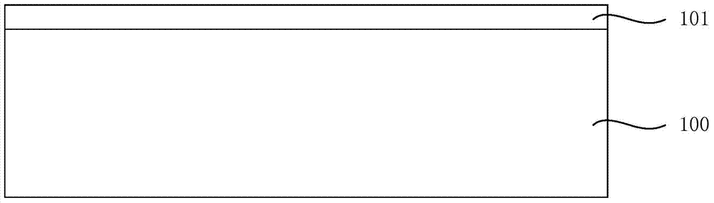
[0042] The manufacture method of the graphene field effect tube provided by the present embodiment comprises:

[0043] A semiconductor substrate is provided, and a silicon dioxide layer is formed on the surface of the semiconductor substrate;

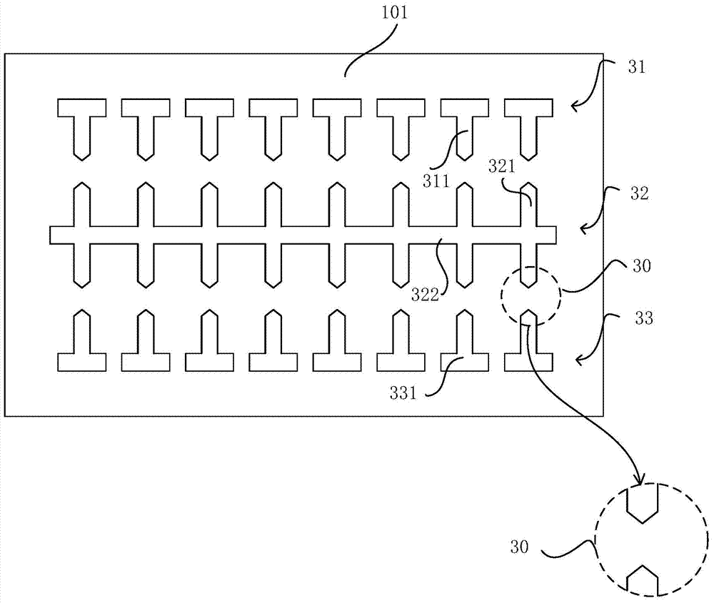
[0044] A floating potential AC dielectrophoretic structure is formed on the semiconductor substrate, and the floating potential AC dielectrophoretic structure includes:

[0045] The first electrode part, the second electrode part and the third electrode part, wherein the first electrode part includes at least a first sub-electrode, the second electrode part includes at least a second sub-electrode and a sub-electrode connection line, and the sub-electrode connection line Connecting through all the second sub-electrodes, the third electrode part includes at least a third sub-electrode, the first sub-electrode and the second sub-electrode, and the top ends of the second sub-electrode and the third sub-electrode are respectively facing eac...


PUM

PropertyMeasurementUnit
frequencyaaaaaaaaaa
diameteraaaaaaaaaa
widthaaaaaaaaaa

Abstract

The invention provides a production method of a graphene field-effect transistor. The production method comprises the steps as follows: a semiconductor substrate with a silicon dioxide layer formed on the surface is provided; a floating potential alternating current dielectrophoresis structure is formed and comprises a first electrode part, a second electrode part and a third electrode part, wherein the first electrode part at least comprises a first sub-electrode, the second electrode part at least comprises a second sub-electrode and a sub-electrode connecting wire, the third electrode part at least comprises a third sub-electrode, the sub-electrode connecting wire is connected with each second sub-electrode in a penetrating manner, and top ends of each second sub-electrode and each third sub-electrode are in one-to-one correspondence; a carbon nanotube suspension is formed; a carbon nanotube is connected between each second sub-electrode and each third sub-electrode which are opposite to each other by utilizing an alternating current dielectrophoresis technology; each carbon nanotube is fixed; metal layers are formed by utilizing a sputtering technology; and metal is removed and graphene nanoribbons are formed. According to the production method, the perfect alignment of single carbon nanotubes is realized in a batch manner, and single-walled carbon nanotubes are cut into graphene nanoribbons, so that the graphene nanoribbons can present typical semiconductor characteristics.

Description

technical field [0001] The invention relates to a semiconductor technology, in particular to a method for manufacturing a graphene field effect tube. Background technique [0002] Graphene is a new carbonaceous material in which a single layer of carbon atoms is tightly packed into a two-dimensional honeycomb lattice structure. It is the basic unit for constructing other dimensional carbonaceous materials (such as fullerenes, carbon nanotubes, and graphite). It has semiconductor electrical characteristics such as high carrier mobility, adjustable bandgap width, and high thermal conductivity. At the same time, its thin film morphology is compatible with the current silicon planar process and can be integrated on a large scale. It may become a new generation that surpasses and replaces silicon-based CMOS. One of the semiconductor materials. However, the zero-bandgap structure of graphene limits its application in the field of electronics. Theoretical and experimental studies...

Claims


Application Information

Patent Timeline
Patent Type & Authority Applications(China)
IPC IPC(8): H01L21/336B82Y40/00
CPCH01L29/1606H01L29/66045
Inventor 王浩敏谢红孙秋娟王慧山吴天如谢晓明
Owner SHANGHAI INST OF MICROSYSTEM & INFORMATION TECH CHINESE ACAD OF SCI
Why Eureka
Try Eureka