Manufacturing method for embedded type semiconductor package piece of element

A manufacturing method and embedded technology, which is applied in semiconductor/solid-state device manufacturing, electrical components, circuits, etc., can solve the problems of carrier board and multilayer circuit board deformation, increase the defect rate of non-core manufacturing process, etc., and achieve simplified manufacturing process, increasing the yield of the manufacturing process, and the effect of thin package thickness

Active Publication Date: 2014-01-01
TRIPOD WUXI ELECTRONICS
View PDF5 Cites 8 Cited by
  • Summary
  • Abstract
  • Description
  • Claims
  • Application Information

AI Technical Summary

Problems solved by technology

[0005] However, in the existing coreless manufacturing process, because the carrier board and the multilayer circuit board are only partially bonded by adhesive, it is easy to generate relative movement in the above-mentioned multi-channel manufacturing process, or the carrier board and the multilayer circuit board Deformation occurs in the unbonded part, which increases the defective rate of coreless manufacturing process

Method used


Image

  • Manufacturing method for embedded type semiconductor package piece of element
  • Manufacturing method for embedded type semiconductor package piece of element
  • Manufacturing method for embedded type semiconductor package piece of element

Examples


Embodiment Construction

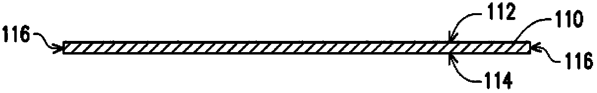
[0054] Figures 1A to 1J It is a schematic cross-sectional view of a manufacturing process of a device-embedded semiconductor package according to an embodiment of the present invention. Please refer to Figure 1A , in this embodiment, the fabrication method of the component-embedded semiconductor package includes the following steps: First, please refer to Figure 1A , a metal substrate 110 is provided. Specifically, the metal substrate 110 has a substrate upper surface 112 and a substrate lower surface 114 opposite to each other, and a substrate side surface 116 connecting the substrate upper surface 112 and the substrate lower surface 114 . In this embodiment, the material of the metal substrate 110 is, for example, aluminum or stainless steel.

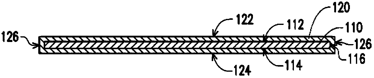
[0055] Next, please refer to Figure 1B , forming a metal layer 120 on the metal substrate 110 , wherein the metal layer 120 completely covers the metal substrate 110 . In this embodiment, the method for forming the metal layer...


PUM

PropertyMeasurementUnit
thicknessaaaaaaaaaa

Abstract

The invention discloses a manufacturing method for an embedded type semiconductor package piece of an element. A metal substrate is provided. A metal layer is formed on the metal substrate and coats the metal substrate. The metal layer is provided with the upper surface, the lower surface and the first side surface, wherein the upper surface and the lower surface are mutually opposite and are connected through the first side surface. A patterning photo-resist layer is formed on the metal layer, and a part of the upper surface and a part of the lower surface are exposed out of the patterning photo-resist layer. A plurality of connecting pads are formed on the portion, exposed out of the patterning photo-resist layer, of the upper surface and the portion, exposed out of the patterning photo-resist layer, of the lower surface, and the patterning photo-resist layer coats second side surfaces of the connecting pads. The second side surfaces of the connecting pads are exposed after the patterning photo-resist layer is removed. A plurality of electronic elements are arranged on the connecting pads. An insulation layer is pressed on the metal layer in a combination mode and coats the electronic elements, the connecting pads and a part of the metal layer.

Description

technical field [0001] The present invention relates to a manufacturing method of a semiconductor package, and in particular to a manufacturing method of a component-embedded semiconductor package. Background technique [0002] In recent years, with the rapid development of electronic technology and the successive advent of high-tech electronic industries, more user-friendly and better-functioning electronic products have been continuously introduced, and are designed towards the trend of light, thin, short and small. In the current semiconductor manufacturing process, the chip package carrier is one of the frequently used package components. The chip package carrier is, for example, a multi-layer circuit board, which is mainly formed by alternately stacking multi-layer circuit layers and multi-layer dielectric layers. [0003] In the above-mentioned multi-layer circuit board, in the past, multi-layer circuits and multi-layer dielectric layers are fabricated on a core subst...

Claims


Application Information

Patent Timeline
Patent Type & Authority Applications(China)
IPC IPC(8): H01L21/56H01L21/60
CPCH01L21/4871H01L21/4825H01L21/561
Inventor 藤川治孙奇杨中贤杨伟雄
Owner TRIPOD WUXI ELECTRONICS
Why Eureka
Try Eureka